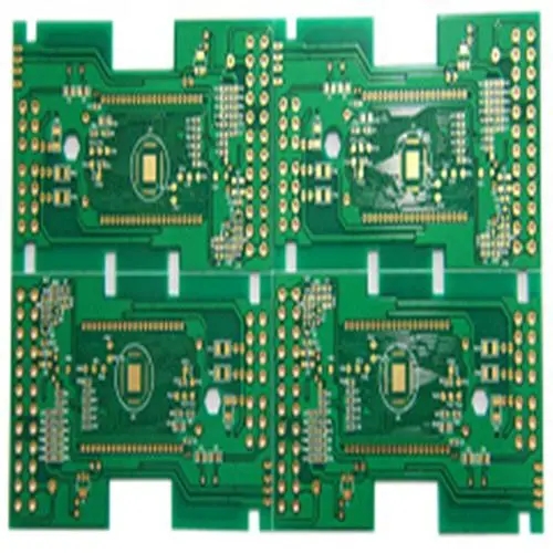
Kingford focus on the high-quality PCBA order demand of "Multiple varieties, medium and small batch, and short lead time".


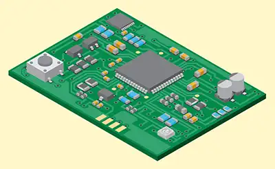
As a PCB and PCB assembly manufacturer, it is necessary to let you know what our PCB assembly servICes are. PCB assembly is a complex and lengthy process involving many different stages and a key process in achieving the functionality of the final product. Every step has to be carried out very carefully. Any small mistakes in the assembly process will lead to the failure of the final assembly. To help you learn more about the entire PCBA process, we explain each step in detail below.
before the assembly process
1. design for Manufacturability (DFM) Inspection
So what is DFM CHECK? Before the actual assembly process, the manufacturer thoroughly examines the PCB design files to check functionality and manufacturability. This phase, which we call DFM, examines the design specifications of the PCB and analyzes any missing, redundant, or potentially problematic features. This stage helps detect design errors and allows designers to remove all defects immediately for successful production.

2. Electronic component inspection
Kingford will do another step before assembly, component inspection, our team of engineers will check whether the component package, value, quantity, package, part number, etc. match the BOM and PCB board. We will work with the customer to resolve any errors before starting assembly.
Actual PCB Assembly Process Steps
1. Solder paste printing
Solder paste printers are designed to apply solder paste (a paste of small particles of solder mixed with flux) onto the appropriate pads on a circuit board using a stencil and a squeegee.
2. Component placement
This stage of the PCB assembly process is now fully automated. The pick and place of components such as surface mount components, once done manually, is now performed by robotic pick and place machines. These machines precisely place components into pre-planned areas of the board.
3. Reflow soldering
Once the solder paste and surface mount components are in place, they need to stay there. This means that the solder paste needs to cure, adhering the components to the board. To do this, the components using the solder paste and the components on it are passed through a conveyor belt that passes through an industrial-grade reflow oven. A heater in the oven melts the solder in the solder paste. Once this melting is complete, the assembly is again moved on a conveyor belt and exposed to a series of cooler heaters. The purpose of these coolers is to cool the molten solder and bring it to a solidified state.

4. Inspection
After the reflow process, the PCB is inspected to check its functionality. This stage helps identify poor quality connections, misplaced components, and shorts due to the continuous movement of the board during reflow. PCB manufacturers employ multiple inspection steps, including visual inspection, automated optical inspection, and X-ray inspection, to check the functionality of circuit boards, identify poor-quality solder, and identify any potential hidden problems.
5. Through-hole component insertion
Certain types of PCBs require insertion of through-hole components as well as the usual SMD components. This stage is dedicated to this type of component insertion. For this purpose, plated-through holes are created with the help of PCB components that pass signals from one side of the board to the other. PCB through hole insertion is usually achieved by hand soldering or wave soldering.
Wave Soldering Manual Soldering
6. Final inspection and functional testing/IC programming
After the soldering step of the PCBA process is complete, a final inspection will test the functionality of the PCB. Such checks are calLED "functional tests". This test simulates normal operation of the PCB by testing the PCB. In this test, power and analog signals pass through the PCB while the tester monitors the electrical characteristics of the PCB.
7. Cleaning and Packaging
Since the soldering process leaves some flux residue in the PCB, it is critical to thoroughly clean the components before shipping the final board to the customer. For this, PCBs are washed in deionized water. After the cleaning process, use compressed air to dry the board thoroughly. The PCB assembly is now ready for customer inspection and inspection.
The advantages and usage rules of rigid-flex PCB
Oct 14,2022


Copyright © 2021-2022 Shenzhen Kingford Technology Co., LTD. All Rights Reserved Sitemap