


Own supporting PCB board factory and patch factory to ensure the cost control of PCB design.
Proper PCB layout & design is vital for your printed circuit board success.
Over 20 years working experience for PCB layout and design.
Over 10 free PCB layout & design software for your projects.
7/24 sales and tech support.
- PCB Assembly Services+-
- BGA Assembly
- SMT Assembly
- LED PCB Assembly
- Rigid-Flex PCB Assembly
- Turnkey PCB Assembly
- Prototype PCB Assembly
- Through Hole PCB Assembly
- Low Volume PCB Assembly
- High Volume PCB Assembly
- Hybrid PCB Assembly
- Single-sided PCB assembly
- Double-Sided PCB Assembly
- SMT chip processing
- DIP plug-in processing
- Medical PCB Assembly
- Industrial PCB Assembly
- Consumer Electronics PCBA
- Automotive Electronics PCBA
- Energy Storage Module PCBA
- Military Applications PCBA
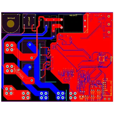
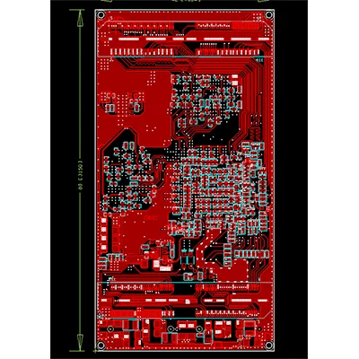
- PCB Manufacturing Services+-
- Electronic Design Services+-
- Standard PCB Design
- HDI PCB Design
- Multilayer PCB Design
- PCB Reverse Engineering
- High speed PCB Design
- High Power PCB Design
- High Voltage PCB Design
- Amplifier PCB Design
- Gold Fingers PCB Design
- Impedance Control PCB Design
- Rigid Flex PCB Design
- Halogen Free PCB Design
- LED PCB Design
- RF PCB Design
- Metal Core PCB Design
- Finished Product Assembly
- Components Purchasing
- DFMA Services
- Finished Product Test
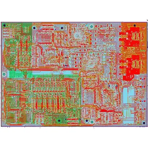
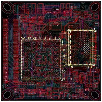
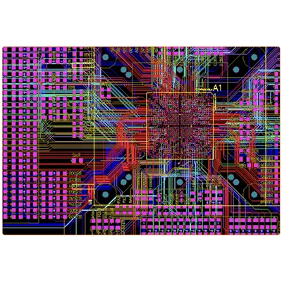
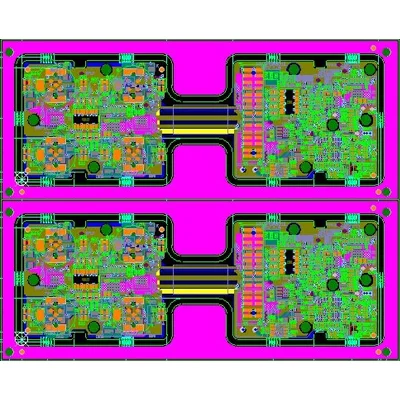
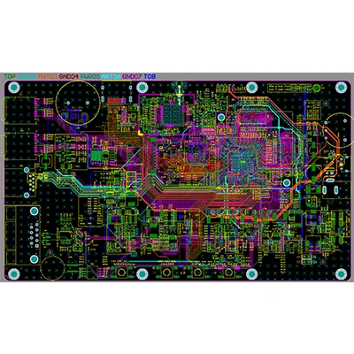
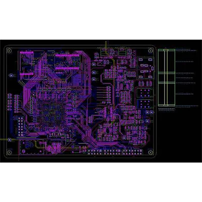
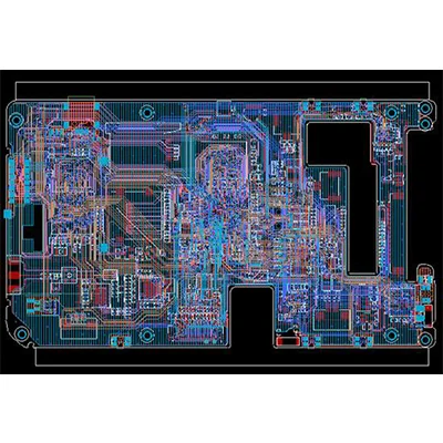
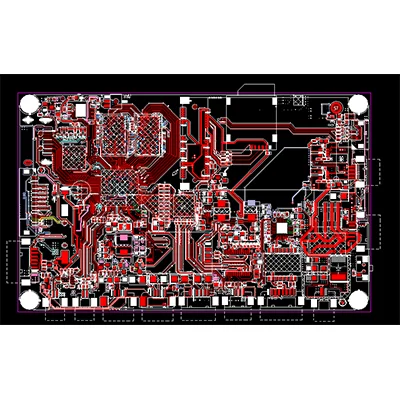
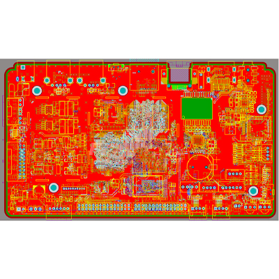
- PCB Design Capabilities
| PCB Design&Layout Capabilities | |||
| Min.trace width: | 2.5mil | Min.trace spacing | 2.5mil |
| Min.Vias: | 6mil(4mil laser drilling) | Max.layer | 48L |
| Min.BGA spacing | 0.35mm | Max.BGA Pin | 3600pin |
| Max.high-speed signal | 40 GBPS | Fastest delivery time | 6 Hours/ Item |
| HDI Highest layer | 22 L | HDI Highest layer | 14 L any layer HDI |
| PCB Design&Layout lead time | |||
| Number of pins on the board | 0-1000 | Design lead time (working days) | 3-5 days |
| 2000-3000 | 5-8 days | ||
| 4000-5000 | 8-12 days | ||
| 6000-7000 | 12-15 days | ||
| 8000-9000 | 15-18 days | ||
| 10000-12000 | 18-20 days | ||
| 13000-15000 | 20-22 days | ||
| 16000-18000 | 22-25 days | ||
| 18000-20000 | 25-30 days | ||
| Ultimate delivery capacity | 10000Pin/7 days | ||
| PS: The above delivery date is the regular delivery date, and the accurate design delivery date needs to be comprehensively evaluated according to the number of components, difficulty, layers and other factors of the circuit board! | |||
Kingford provides Consumer Electronics RF PCB Design services. This is a PCBA one-stop assembly fact...
We provide xx services. Kingford is your one stop turnkey PCB assembly factory. Looking forward to y...
RF printed circuit boards are also capable of supporting high bandwidth transmission of data systems...
Motor vehicles require improved electrical performance. The automotive industry is also regulated to...
RF PCBs have been used in the medical industry for some time. Typically, medical equipment such as X...
RF PCBs have been used in the medical industry for some time. Typically, medical equipment such as X...
