

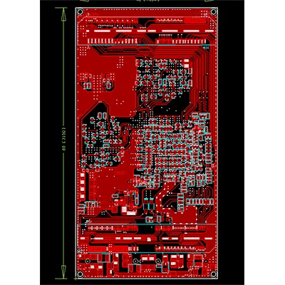
Consumer Electronics RF PCB Design
Name: Consumer Electronics RF PCB Design
Designable layers: 1-32 layers
Minimum line width and line spacing: 3mil
Minimum laser aperture: 4mil
Minimum mechanical aperture: 8mil
Copper foil thickness: 18-175цm (standard: 18цm35цm70цm)
Peel strength: 1.25N/mm
Minimum punching hole diameter: single side: 0.9mm/35mil
Minimum hole diameter: 0.25mm/10mil
Aperture tolerance: ≤φ0.8mm±0.05mm
Hole tolerance: ±0.05mm
Hole wall copper thickness: double-sided/multi-layer: ≥2um/0.8mil
Hole resistance: double-sided/multi-layer: ≤300цΩ
Minimum line width: 0.127mm/5mil
Minimum pitch: 0.127mm/5mil
Screen printing color: black, white, red, green, etc.
Surface treatment: lead/lead-free tin spray, ENIG, silver, OSP
Service: Provide OEM service
Certificate: ISO9001.ROSH.UL
Radio frequency technology (RF) is the abbreviation of Radio Frequency. The more common applications are Radio Frequency Identification (RFID), often called inductive electronic chips or proximity cards, proximity cards, contactless cards, electronic tags, electronic barcodes, etc. The principle is that the scanner transmits radio wave energy of a specific frequency to the receiver, which is used to drive the receiver circuit to send out the internal code, and the scanner then receives the code.
The special feature of the receiver is that it does not need batteries, no contact, and no card swiping, so it is not afraid of dirt, and the chip password is the only one in the world that cannot be copied, with high security and long life. The application of RFID is very extensive. At present, typical applications include animal chips, car chip anti-theft devices, access control, parking lot control, production line automation, and material management.
There are two types of RFID tags: active tags and passive tags.
The basic model of the RFID system is shown in the figure.
Among them, electronic tags are also called radio frequency tags, transponders, and data carriers; readers are also called readout devices, scanners, communicators, and readers (depending on whether the electronic tags can rewrite data wirelessly). The space (non-contact) coupling of radio frequency signals is realized between the electronic tag and the reader through the coupling element, and in the coupling channel, energy transmission and data exchange are realized according to the timing relationship.
There are two types of coupling of RF signals that occur between the reader and the tag.
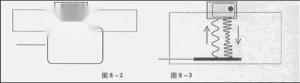
(1) Inductive coupling. The transformer model realizes coupling through the space high-frequency alternating magnetic field, based on the law of electromagnetic induction, as shown in the figure:
(2) Electromagnetic backscatter coupling: the radar principle model, the emitted electromagnetic waves are reflected after hitting the target, and carry back the target information at the same time, based on the spatial propagation law of electromagnetic waves.
The inductive coupling method is generally suitable for short-range RFID systems with low and high frequency operations. Typical operating frequencies are: 125kHz, 225kHz and 13.56MHz. The recognition distance is less than 1m, and the typical distance is 10-20cm.
The electromagnetic backscatter coupling method is generally suitable for long-distance radio frequency identification systems that work with UHF and microwave. Typical operating frequencies are: 433MHz, 915MHz, 2.45GHz, 5.8GHz. The recognition distance is greater than 1m, and the typical distance is 3-l0m.
Kingford provides Consumer Electronics RF PCB Design services. This is a PCBA one-stop assembly factory with senior industry experience. Welcome to know us.
Name: Consumer Electronics RF PCB Design
Designable layers: 1-32 layers
Minimum line width and line spacing: 3mil
Minimum laser aperture: 4mil
Minimum mechanical aperture: 8mil
Copper foil thickness: 18-175цm (standard: 18цm35цm70цm)
Peel strength: 1.25N/mm
Minimum punching hole diameter: single side: 0.9mm/35mil
Minimum hole diameter: 0.25mm/10mil
Aperture tolerance: ≤φ0.8mm±0.05mm
Hole tolerance: ±0.05mm
Hole wall copper thickness: double-sided/multi-layer: ≥2um/0.8mil
Hole resistance: double-sided/multi-layer: ≤300цΩ
Minimum line width: 0.127mm/5mil
Minimum pitch: 0.127mm/5mil
Screen printing color: black, white, red, green, etc.
Surface treatment: lead/lead-free tin spray, ENIG, silver, OSP
Service: Provide OEM service
Certificate: ISO9001.ROSH.UL
- Previous:RF Printed Circuit Board Design
- Next:No
