Because copper tends to exist in the form of oxides in the air, which seriously affects the solderability and electrical properties of the PCB, the PCB needs to be surface treated. If the surface of the circuit board is not treated, it is easy to produce soldering problems, and in severe cases, the pads and components cannot be soldered. The PCB surface treatment refers to the process of artificially forming a surface layer on the PCB. The purpose of surface treatment is to ensure good solderability or electrical properties of the PCB. There are many types of surface treatments for printed circuit boards.
1. Hot air solder leveling (Known as HASL)
It is a process of coating molten tin-lead solder on the surface of the PCB and flattening (blowing) it with heated compressed air to form a coating layer that not only resists copper oxidation but also provides good solderability. In this process, the following important parameters need to be mastered: welding temperature, air knife air temperature, air knife pressure, dip soldering time, lifting speed, etc.
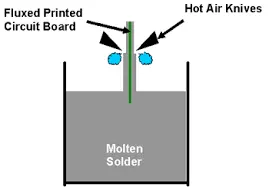
Hot air leveling is now widely used in the SMT process.There are three main points when PCB leveling with hot air:
The PCB should be immersed in molten solder;
The wind knife blows the liquid solder before the solder solidifies;
The wind knife can minimize the meniscus of the solder on the copper surface And prevent solder bridging.
Advantages of HASL
Relatively long storage time.
Good pad wetting and copper coverage.
Lead free (RoHS compliant) variant widely available.
Mature technology.
Low cost.
Highly suited for visual inspection and electrical testing.
Disadvantages of HASL
Not suitable for wire bonding.
Poor planarity due to the natural meniscus of molten solder.
Not suitable for capacitive touch switches.
For particularly thin panels, HASL may not be suitable. The high heat of the bath may cause board warping.
2.OSP (organic protective film)
OSP is the abbreviation of Organic Solderability Preservatives, also known as Preflux. In a nutshell, OSP is sprayed onto the surface of the copper pads to provide a protective film made of organic chemicals. This layer of the film must have the characteristics of oxidation resistance, heat shock resistance, moisture resistance, etc., to protect the copper surface from rusting (oxidation or vulcanization, etc.) in a normal environment. However, in the subsequent high temperature soldering, this protective film must be easily removed by the flux quickly, so that the exposed clean copper surface can be immediately combined with the molten solder to form a strong solder joint in a very short time. In other words, the role of OSP is to act as a barrier between copper and air.
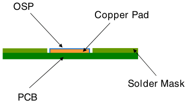
The general process of OSP is: degreasing –> microetching –>acid cleaning –> pure water cleaning –> organic coating –> cleaning.
Advantages of OSP
Simple and cheap; surface finish is just sprayed on.
Pad surface is very smooth, planarity comparable to ENIG.
Lead free (RoHS compliant) and environmentally friendly.
Reworkable.
Disadvantages of OSP
Poor wettability.
Clear and thin nature of the film means it is difficult to gauge quality with visual inspection and perform in-circuit testing.
Poor lifetime, high storage and handling requirements.
Poor protection for plated through holes.
3.Immersion silver
Silver has stable chemical properties. Even if the PCB processed by the immersion silver process is exposed to heat, humidity and pollution, it can still provide good electrical properties and maintain good solderability, even if it will lose its luster. Immersion silver is a displacement reaction, directly coating copper with a layer of pure silver. Sometimes immersion silver is combined with a coating of OSP to prevent the silver from reacting with sulfides in the environment.
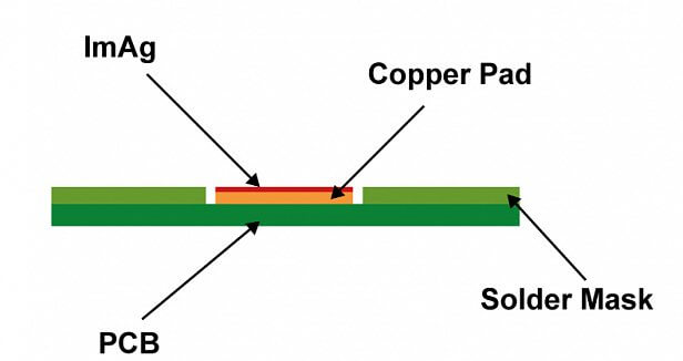
Advantages of Immersion Silver
High solderability.
Good surface planarity.
Low cost and lead free (RoHS compliant).
Suitable for aluminum wire bonding.
Disadvantages of immersion silver
High storage requirements. Easily contaminated.
Short assembly window once removed from packaging.
Hard to electrically test.
4.Immersion Tin
Since all solders are tin-based, the tin layer can match any type of solder. After adding organic additives to the tin immersion solution, the tin layer structure takes a granular structure, which overcomes the problems caused by the migration of tin whiskers and tin, and also has good thermal stability and solderability.
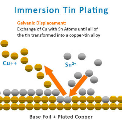
Advantages of immersion tin
Suitable for horizontal production line.
Suitable for fine trace processing, suitable for lead-free soldering, especially for crimping technology.
Very good flatness, suitable for SMT.
Disadvantages of immersion tin
High storage conditions, tarnishing can occur from fingerprints.
Tin whiskers may cause shorts and solder joint issues therefore shelf life is reduced.
Hard to electrically test.
Process involves a carcinogen.
5. Immersion Gold (ENIG)
ENIG, or Electroless Nickel Immersion Gold is a widely-used surface treatment coating, consisting of two metallic layers. Nickel is deposited directly onto the copper which is then coated in gold atoms via a displacement reaction. The thickness of the inner layer of Ni is generally 3~6μm, and the deposition thickness of the outer layer of Au is generally 0.05~0.1μm. Ni forms a barrier layer between solder and copper. The role of Au is to prevent Ni oxidation during storage, resulting in a long shelf-life but the immersion gold process also produces excellent surface planarity.
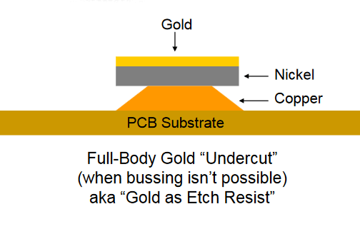
ENIG’s treatment process is as follows: cleaning –>etching –> catalyst –> electroless nickel plating –> immersion gold –> cleaning residue
Advantages of Immersion Gold (ENIG)
Suitable for lead-free (RoHS compliant) soldering.
Excellent surface planarity.
Long shelf-life, surface is durable.
Suitable for aluminum wire bonding.
Disadvantages of Immersion Gold (ENIG)
Expensive, uses gold.
The process is complicated and difficult to control.
Prone to black pad effect.
6. Electrolytic Nickel/Gold (Hard Gold/Soft Gold)
Electrolytic nickel gold is divided into “hard gold” and “soft gold”. Hard gold has a lower purity and is commonly used for gold fingers (PCB edge connectors), PCB contacts or other hard-wear areas. Gold thicknesses may vary according to requirements. Soft gold is purer and is often used in wire bonding applications.
Advantages of Electrolytic Nickel/Gold
Longer shelf life.
Suitable for contact switches and wire bonding.
Hard gold is suitable for electric test.
Lead-free (RoHS compliant).
Disadvantage of Electrolytic Nickel/Gold
Most expensive surface finish.
Electroplating gold finger requires an additional conductive trace.
Hard gold has poor solderability. Due to the thickness of the gold, thicker layers are more difficult to solder to.
7. ENEPIG
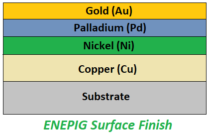
Electroless Nickel Electroless Palladium Immersion Gold, or ENEPIG, is beginning to be used more and more as a PCB surface finish. Compared with ENIG, ENEPIG has an extra layer of palladium between nickel and gold which further protects the nickel layer from corrosion, preventing black pad that may occur with the ENIG finish. The deposition thickness of Ni is about 3~6μm, the thickness of palladium is about 0.1~0.5μm, and the thickness of gold is 0.02~0.1μm. Although the thickness of the gold layer is less than that of ENIG, ENEPIG is more expensive. Recent falls in the cost of palladium have made ENEPIG more affordable however.
Advantages of Nickel palladium (ENEPIG)
All the benefits of ENIG without black pad problems.
More suitable for wire bonding than ENIG.
No corrosion risk.
Long storage time.Lead free (RoHS compliant).
Disadvantages of Nickel palladium (ENEPIG)
Complex process.
Hard to control.
High cost.
ENEPIG is a relatively new method and not mature.


