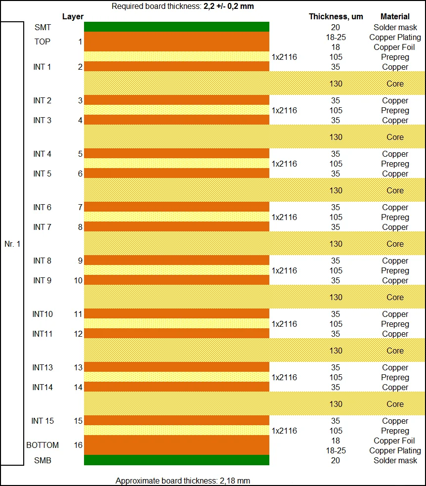
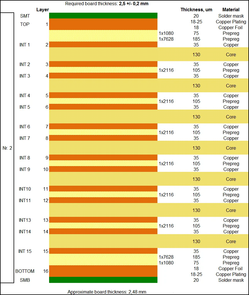
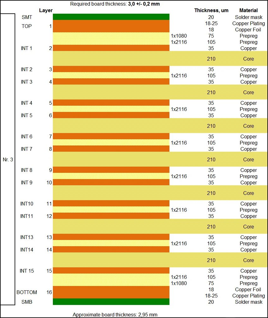
4-16 Layer PCB Stackup
There is really no limit to the number of layers that can be fabricated in a multilayer PCB. Of course, the board thickness increases as the layer count goes up to accommodate the minimum thickness of materials used. Also the aspect ratio (board thickness to smallest hole diameter) has to be considered. Generally this is 10:1 for boards thicker then 100MIL.Kingford can fabricate up to 40 layer PCB boards.
4 Layer PCB Stackup
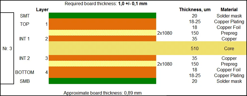
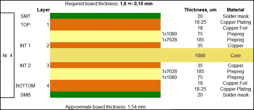
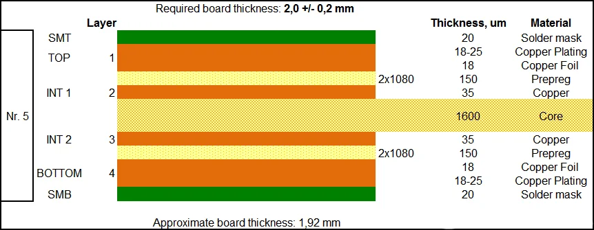
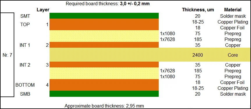
A typical 4 layer PCB board stackup includes two routing layers and two internal planes, one for ground and the other for power.
It is common to see 4 layer boards stacked evenly. Another common mistake is to have the planes closely coupled in the centre with large dielectrics between the signal layers and planes.
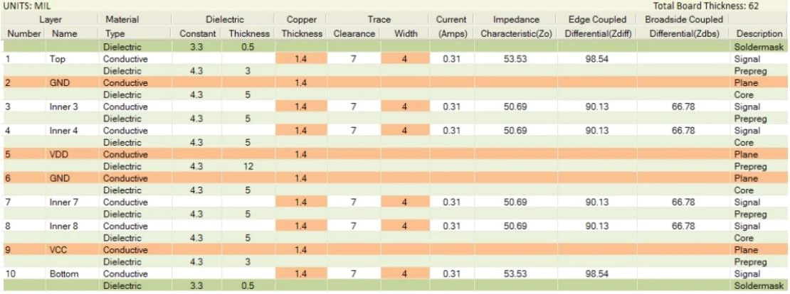
To improve the EMC performance of a 4 layer PCB board, it is best to space the signal layers as close to the planes as possible (< 10 MIL), and use a large core (~ 40 MIL) between the power and ground plane keeping the overall thickness of the substrate to ~ 62 MIL.
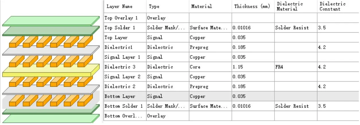
4 Layer PCB Stackup from



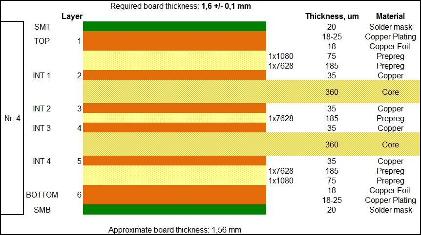
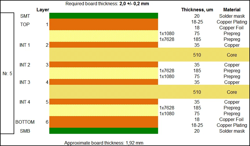
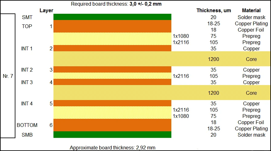
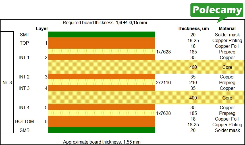
6 Layer PCB Stackup
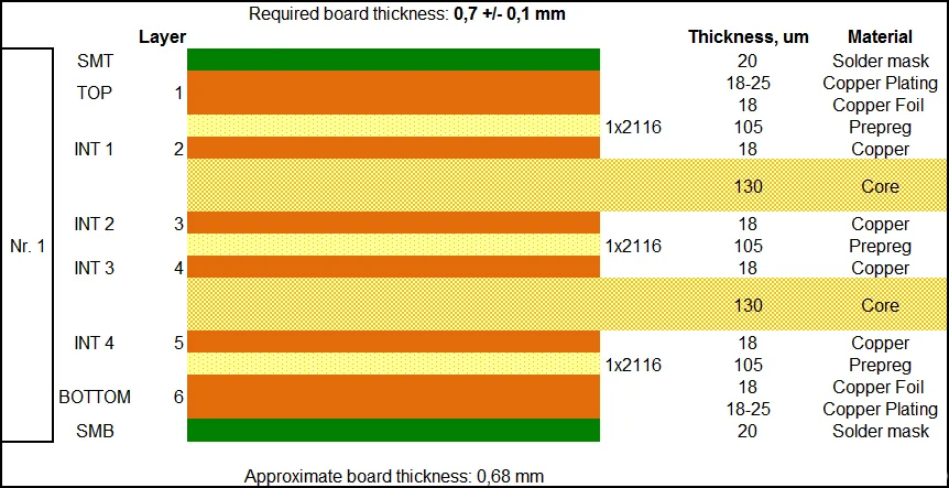
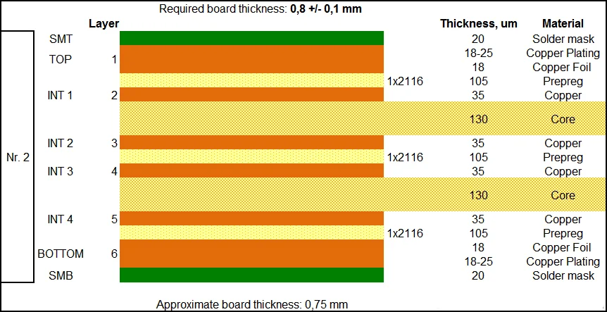
The classic 6 layer PCB stackup includes 4 routing layers (two outer and two internal) and two internal planes (one for ground and the other for power). This improves the EMI dramatically as it provides two buried layers for high-speed signals and two surface layers for routing low speed signals.
6 Layer PCB Stackup from



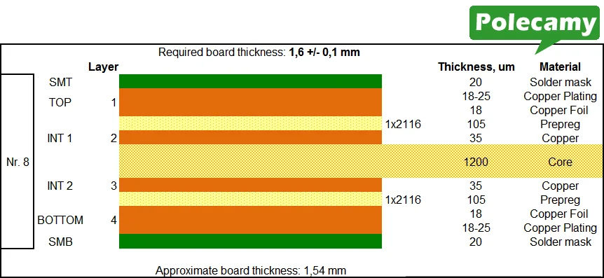
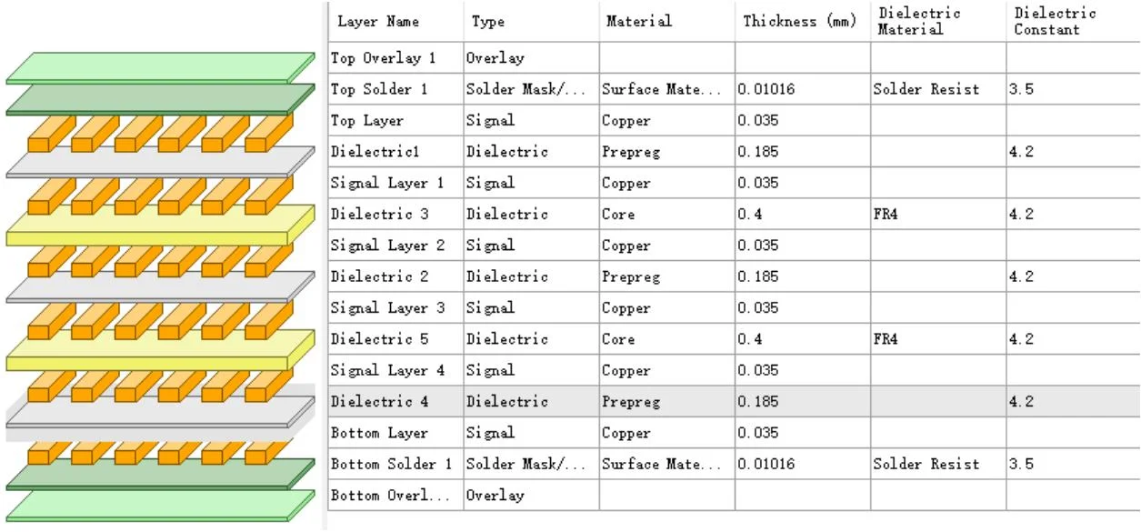
8 Layer PCB Stackup
To improve EMC performance, add two more planes to the 6 layer PCB stackup. It is not recommended to have more then two adjacent signal layers between the planes as this creates impedance discontinuities (~20 ohms difference in impedance of signal layers) and increases crosstalk between these signal layers.
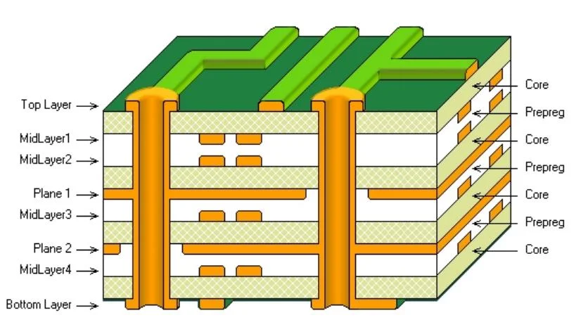
8 Layer PCB Stackup

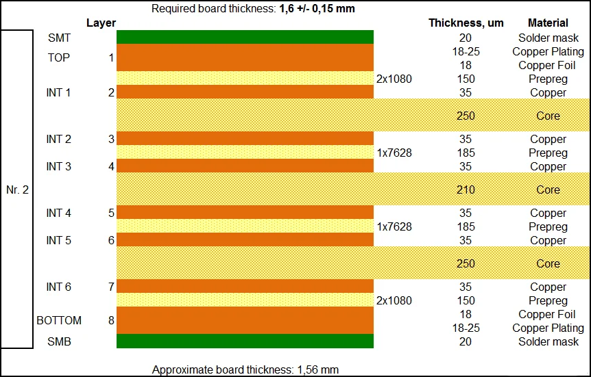
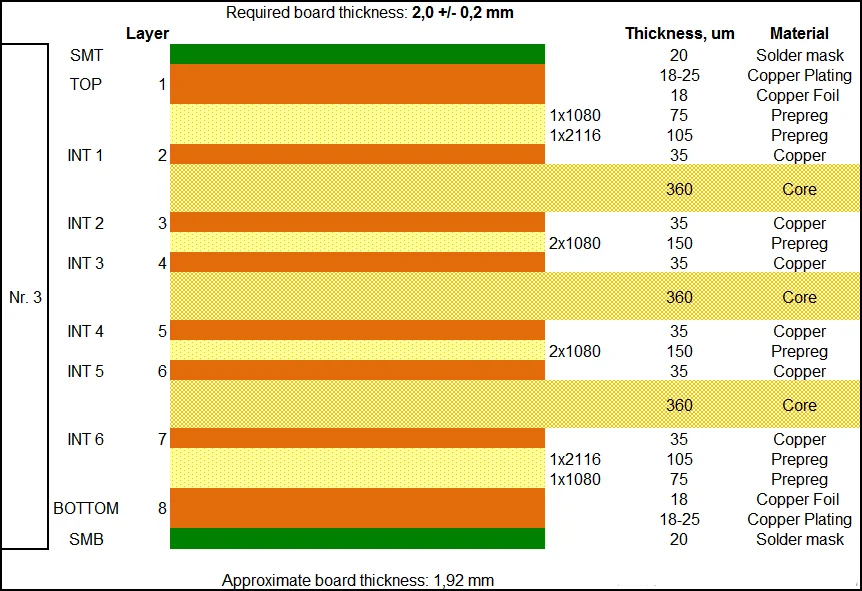
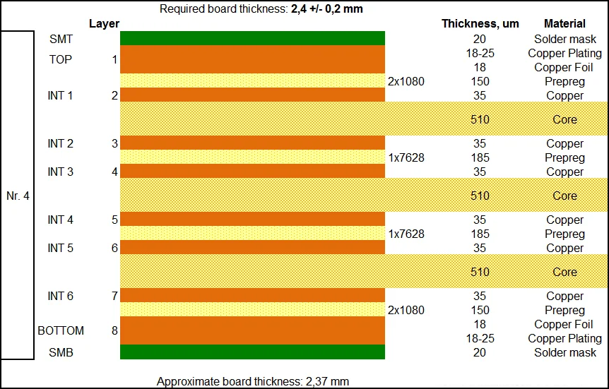
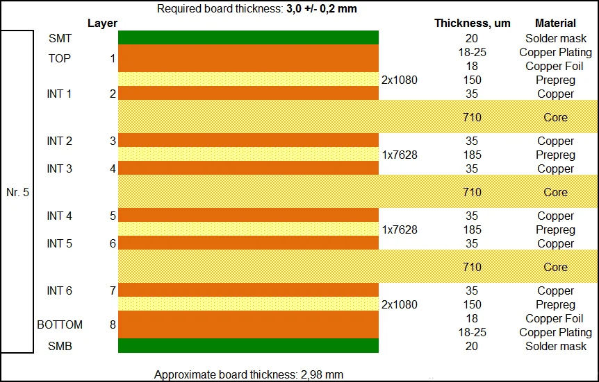
10 Layer PCB Stackup
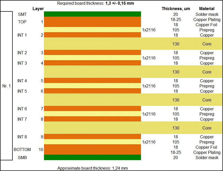
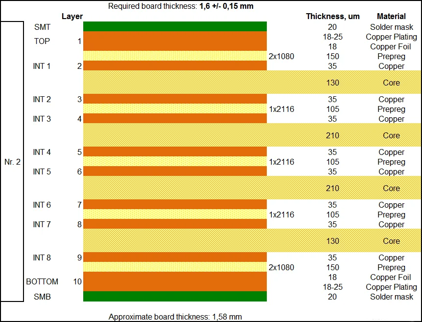
A 10 layer PCB board should be used when 6 routing layers and 4 planes are required and EMC is of concern. This typical 10 layer PCB stackup is ideal because of the tight coupling of the signal and return planes, the shielding of the high speed signal layers, the existence of multiple ground planes, as well as a tightly coupled power/ground plane pair in the center of the board. High speed signals normally would be routed on the signal layers buried between planes (layers 3-4 and 7-8 in this case).
10 Layer PCB Stackup


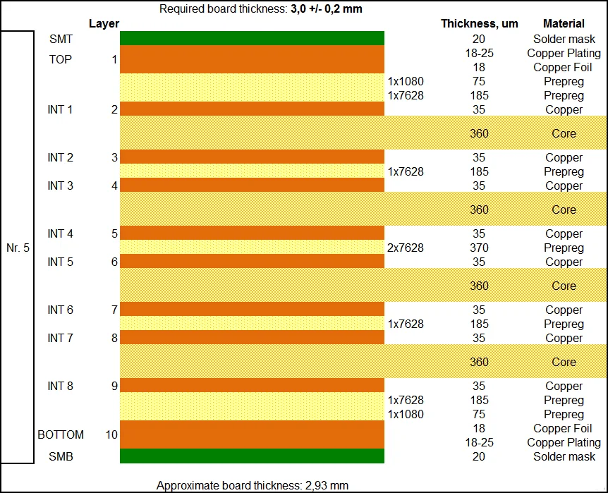
12 Layer PCB Stackup
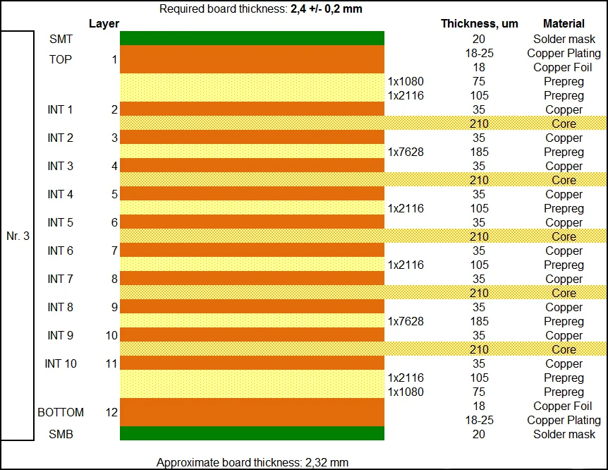
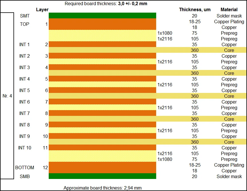
12 layers is the largest number of layers that can usually be conveniently fabricated in a 62MILthick board. Occasionally you will see 14 to 16 layer boards fabricated as a 62MIL thick board,but the numbers of fabricators capable of producing them are limited to those that can produceHDI boards.
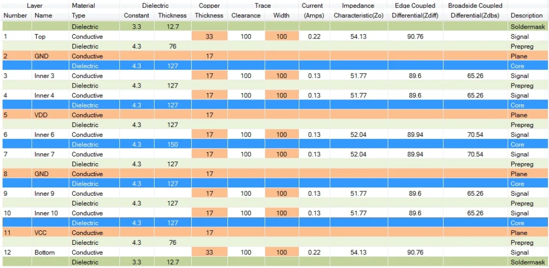
12 Layer PCB Stackup
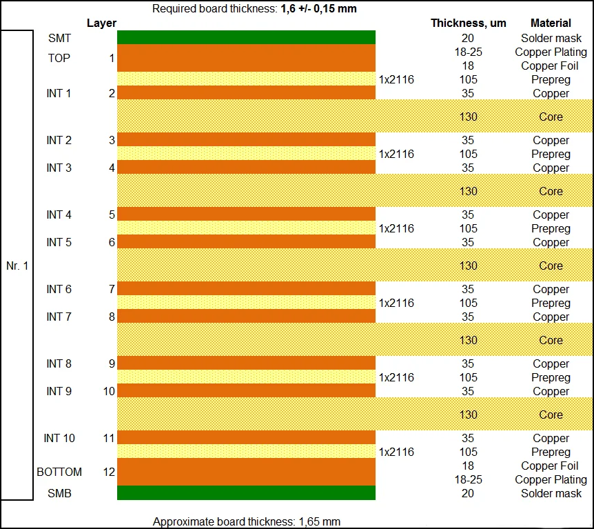
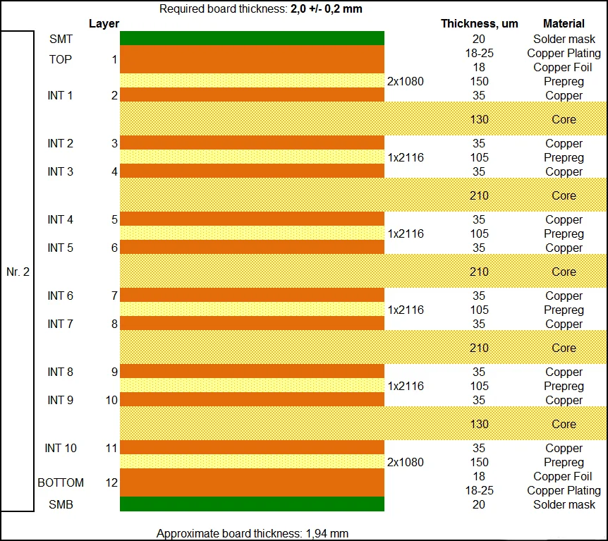
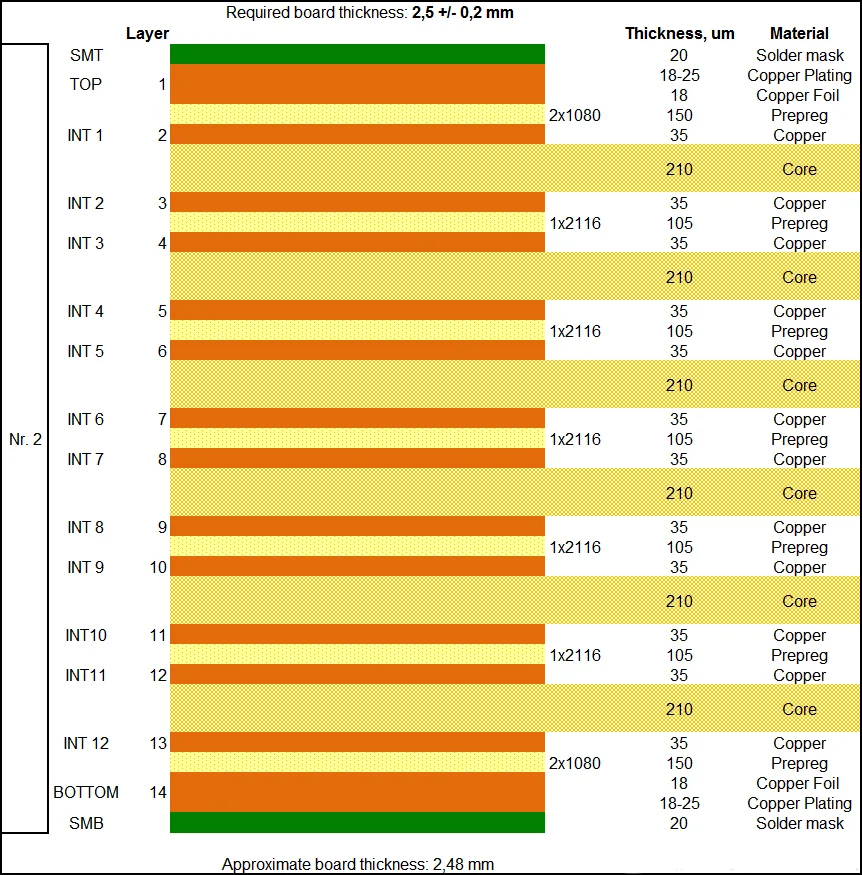
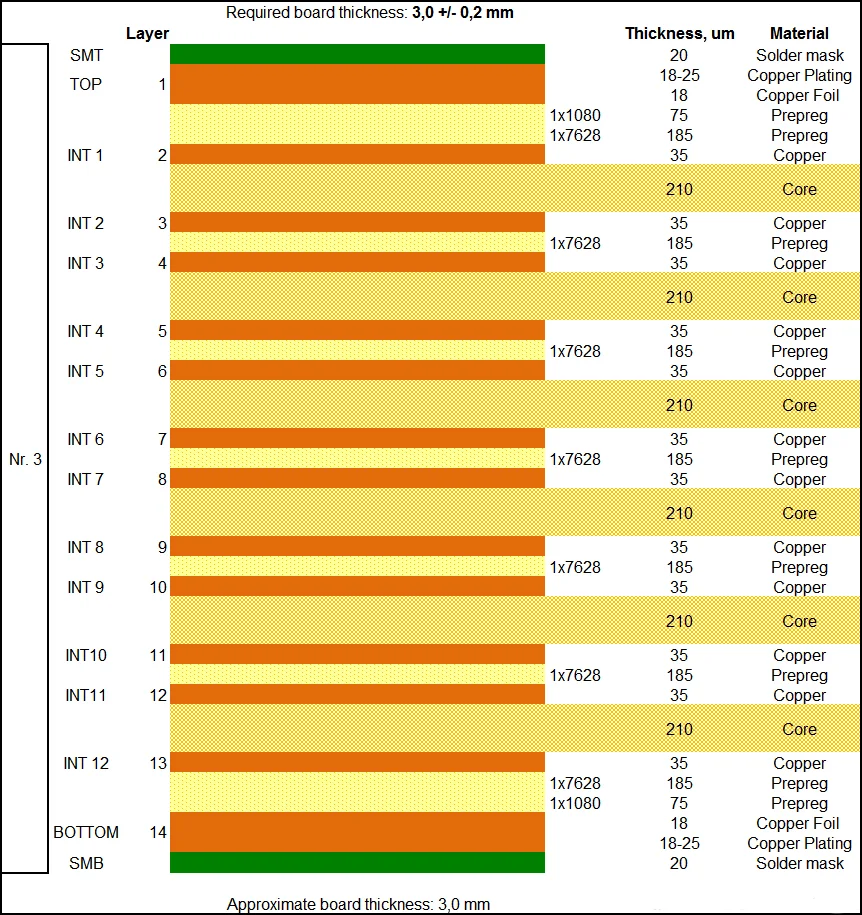
14 Layer PCB Stackup
The 14 layer PCB stackup is used when 8 routing (signal) layers are required plus special shield of critical nets is required. Layers 6 and 9 provide isolation for sensitive signals while layers 3 & 4 and 11 & 12 provide shielding for high speed signals.
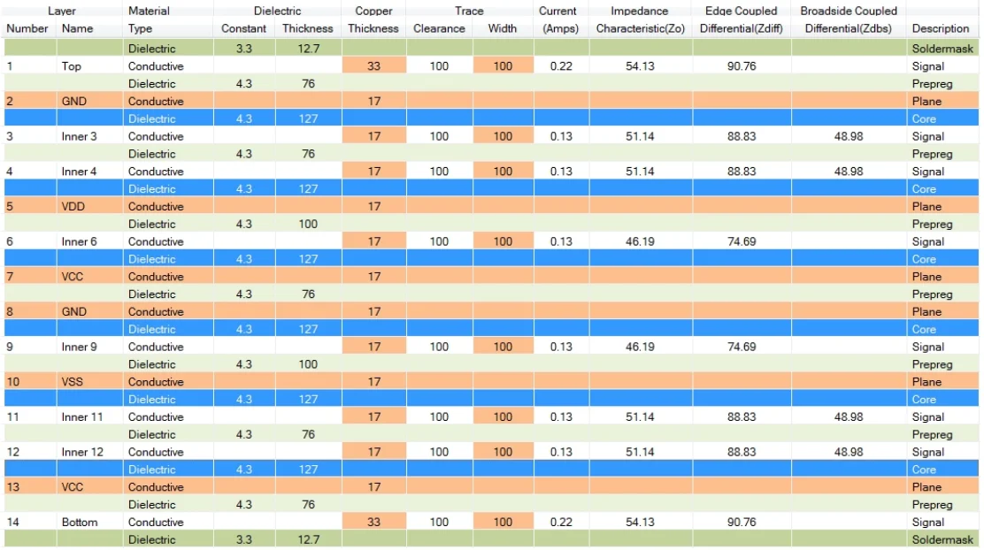
14 Layer PCB Stackup
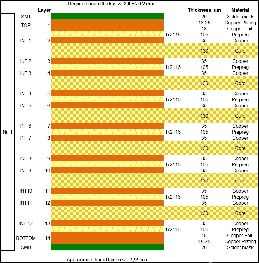
16 Layer PCB Stackup
A 16 layer PCB provides 10 layers of routing and is normally used for extremely dense designs. Generally, you see 16 layer PCBs where the routing technology used in the EDA application.
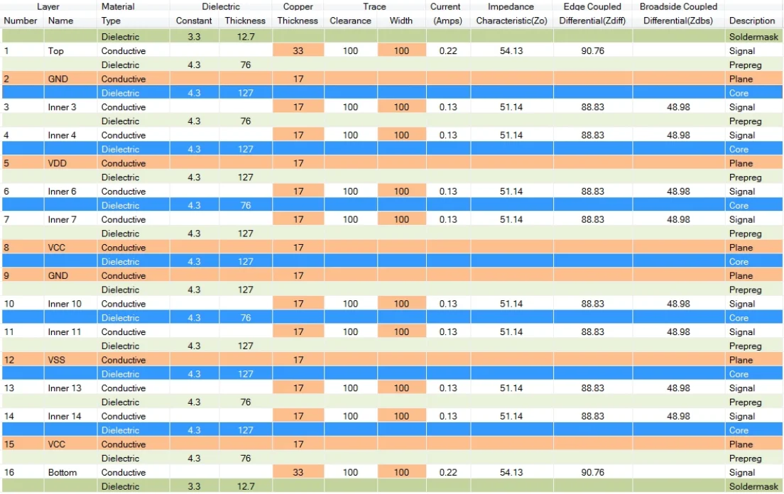
16 Layer PCB Stackup
