

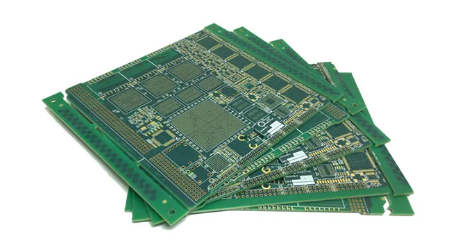
1-40layer board from rigid PCB, rigid-flex PCB, and flexible PCB.
Quick turn order in 24h for prototype PCB.
Working time to follow your local time.
No minimum order quantity, even 1 piece.
7/24 live sales and engineering support.
Sufficient raw materials in stock including KB, Shengyi, Rogers, Arlon, Nelco.
- PCB Assembly Services+-
- BGA Assembly
- SMT Assembly
- LED PCB Assembly
- Rigid-Flex PCB Assembly
- Turnkey PCB Assembly
- Prototype PCB Assembly
- Through Hole PCB Assembly
- Low Volume PCB Assembly
- High Volume PCB Assembly
- Hybrid PCB Assembly
- Single-sided PCB assembly
- Double-Sided PCB Assembly
- SMT chip processing
- DIP plug-in processing
- Medical PCB Assembly
- Industrial PCB Assembly
- Consumer Electronics PCBA
- Automotive Electronics PCBA
- Energy Storage Module PCBA
- Military Applications PCBA
- PCB Manufacturing Services+-
- Electronic Design Services+-
- Standard PCB Design
- HDI PCB Design
- Multilayer PCB Design
- PCB Reverse Engineering
- High speed PCB Design
- High Power PCB Design
- High Voltage PCB Design
- Amplifier PCB Design
- Gold Fingers PCB Design
- Impedance Control PCB Design
- Rigid Flex PCB Design
- Halogen Free PCB Design
- LED PCB Design
- RF PCB Design
- Metal Core PCB Design
- Finished Product Assembly
- Components Purchasing
- DFMA Services
- Finished Product Test
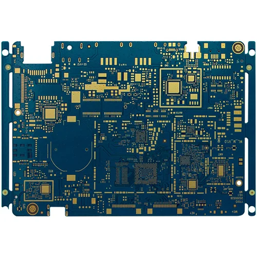
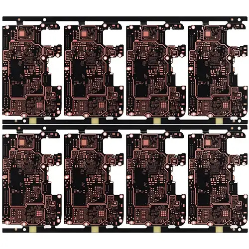
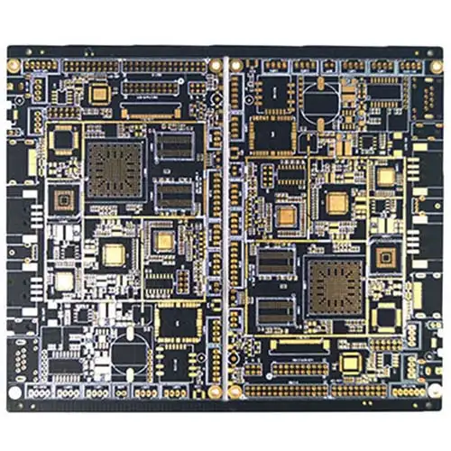
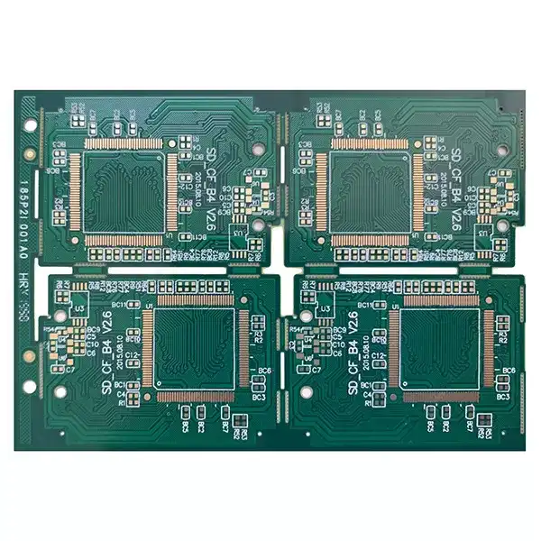
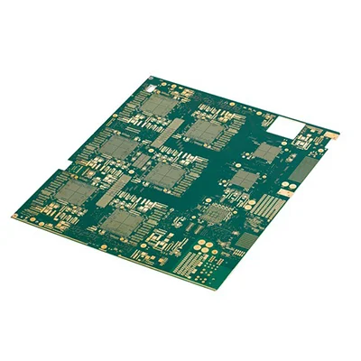
As a leading and professional printed circuit board manufacturing supplier in China, kingford can help you solve all PCB problems, from single layer to 64 layers, from flexible to rigid-flex PCB, from prototype PCB to mass production, kingford is your best Choose one. We can provide fast turnaround service for prototype PCB manufacturing and batch PCB manufacturing, our fastest lead time is 48 hours for prototype manufacturing from single layer to 10 layers, and our fastest lead time for double-sided batch manufacturing to 8 layers is 96 hours.
- PCB Manufacturing Equipment
- PCB Fabrication Capability

PCB Drilling machine

PCB pattern plating line

PCB solder mask expose machine

PCB pattern expose machine

Strip film etching line

Solder mask screen silk print machine

Solder mask scrubbing line
")
PCB Flying Probe Test (FPT)

Fully automatic exposure machine
| Item | Manufacturing Capability |
| PCB Layers | 1~64 Layer |
| Quality Grade | IPC Class 2|IPC Class 3 |
| Laminate/Base material | FR-4|S1141|High Tg|PTFE|Ceramic PCB|Polyimide|S1000-2|IT180A|Isola-FR408HR|FR406|Isola 370 HR|Rogers|Taconic|Arlon|Halogen Free, etc. |
| Brand of Laminate | Kingboard|ITEQ|Shengyi|Nanya|Isola|TUC|SYL|Arlon|Nelco|Taconic|Hitachi|Rogers, etc. |
| High Temperature Material | Normal Tg: Shengyi S1141|KB6160|Huazhen H140(not suitable for lead-free process ) |
| Middle Tg: For HDI、multilayers: SY S1000H|ITEQIT158|HuazhengH150|TU-662|SY S1150G|HuazhengH150HF|H160HF; | |
| High Tg: For thick copper、high layer: SY S1000-2|ITEQIT180A|HuazhengH170|ISOLA: FR408R|370HR|TU-752|SY S1165 | |
| High Frequency Circuit Board Material | Rogers|Arlon|Taconic|SY SCGA-500|S7136|HuazhengH5000 |
| High Speed PCB Material | SY S7439|TU-862HF|TU-872SLK|ISOLA: I-Speed, I-Tera@MT40|Huazheng:H175|H180|H380 |
| Ink | Taiyo INK (Japan)|KUANGSHUN(China)|RONGDA(China)|Coates Screen(UK)|S.M Materials(Taiwan, China) |
| Heat Conductivity for Alu. Boards | 1.0 |
| Chemical | Rohm&Haas (US)|Atotech (Germany)|Umicore (Germany) |
| PCB Type and Services | Prototype PCB|Rigid PCB|Flexible PCB(FPC)|Rigid-Flex PCB|HDI PCB|High Tg PCB|BGA PCB|Impedance Control PCB|IMS PCB(LED PCB Board, Aluminum PCB, Metal Core PCB)|Multilayer PCB|PCBA(PCB Assembly Service) |
| Max Board Size | 609 * 889 mm |
| Board Thickness | 0.1~8.0mm |
| Board Thickness Tolerance | ±0.1mm / ±10% |
| Min base copper thickness | Outer layer:1/3oz (12um) ~10oz|Inner layer:1/2oz~6oz |
| Max finished copperthickness | 6 OZ |
| Min Mechanical Drilling Hole Size | 6mil(0.15mm) |
| Min Laser Drilling Hole Size | 3mil(0.075mm) |
| Min CNC Drilling Hole Size | 0.15mm |
| Hole Wall Roughness(Max) | 1.5mil |
| Min trace width/spacing(Inner Layer) | 2/2mil(Outer layer:1/3oz,Inner layer:1/2oz) (H/H OZ base copper) |
| Min trace width/spacing(Outer Layer) | 2.5/2.5mil (H/H OZ base copper) |
| Min spacing between hole to inner layer conductor | 6mil |
| Min spacing between hole to outer layer conductor | 6mil |
| Min annular ring for via | 3mil |
| Min annular ring for component hole | 5mil |
| Min BGA diameter | 8mil |
| Min BGA pitch | 0.4mm |
| Min Finished hole size | 0.15mm(CNC)|0.1mm(Laser) |
| Half Hole Diameter | Minimum Half hole Diameter: 1mm, Half hole is a special technology, so half hole diameter should be greater than 1mm. |
| Hole Wall Copper Thickness (Thinnest) | ≥0.71mil |
| Hole Wall Copper Thickness (Average) | ≥0.8mil |
| Minimum Air Gap | 0.07mm(3mil) |
| Fine SMD Pitch | 0.07mm(3mil) |
| Max aspect ratios | 20:01 |
| Min soldermask bridge width | 3mil |
| Soldermask/circuit processing method | Film|LDI |
| Min thickness for insulating layer | 2mil |
| HDI & special type PCB | HDI(1-3 steps)|R-FPC(2-16 layers)|High frequency mix-pressing(2-14 layers)|Buried capacitance & resistance … |
| Max. PTH (Round Hole) | 8mm |
| Max. PTH (Round Slot Holes) | 6*10mm |
| PTH Deviation | ±3mil |
| PTH Deviation (Width) | ±4mil |
| PTH Deviation (Length) | ±5mil |
| NPTH Deviation | ±2mil |
| NPTH Deviation (Width) | ±3mil |
| NPTH Deviation (Length) | ±4mil |
| Hole Position Deviation | ±3mil |
| Character Types | Serial Number|Barcode|QR Code |
| Min Character Width (Legend) | ≥0.15mm, Characters width less than 0.15mm will be unidentifiable. |
| Min Character Height (Legend) | ≥0.8mm, Characters height less than 0.8mm will be unidentifiable. |
| Character Width to Height Ratio (Legend) | 1:5, 1:5 is the most suitable ratio for production. |
| Distance between Trace and Outline | ≥0.3mm(12mil), Ship as individual boards: Distance between Trace and Outline ≥0.3mm, Ship as Panelized boards with V-cut: Distance between Trace and V-cut line ≥0.4mm |
| Panelization without Spacing | 0mm, Ship as Panelized boards and the spacing between boards is 0mm. |
| Panelization with Spacing | 1.6mm, Make sure the spacing between boards should be ≥1.6mm, otherwise it will be hard to process routing. |
| Surface Finishes | OSP|HASL|HASL Lead-Free (HASL LF)|Immersion Silver|Immersion Tin|Plated Gold|Immersion Gold(ENIG)|ENEPIG|Golden Finger+HASL|ENIG+OSP|ENIG+Golden Finger|OSP+Golden Finger, etc. |
| Solder-Mask Finishing | (1). Wet Film (LPI Soldermask) |
| (2). Peelable Soldermask | |
| Solder Mask Colors | Green|Red|White|Black, Blue|Yellow|Orange|Purple, Gray|Transparent .etc. |
| Matte: Green|Blue|Black, etc. | |
| Silkscreen Colors | Black|White|Yellow, etc. |
| Electrical Testing | Fixture / Flying Probe |
| Other Testing | AOI, X-Ray(AU&NI), Two-dimension Measurement, Hole Copper Instrument, Controlled Impedance Test(Coupon test&Third Party Report), Metalloscope, Peeling Strength Tester, Solderability Test, Logic Contamination Test |
| Profile | (1). CNC Routing (±0.1mm) |
| (2). CNC V-Cut(±0.05mm) | |
| (3). Bevelling | |
| (4). Mould-Die Punching(±0.1mm) | |
| Special Capabilities | Thick Copper, Thick Gold(5U”), Gold Finger, Blind and Buried Hole, Countersink Hole, Semi-hole, Peelable Mask, Carbon Ink, Counter sink hole, Plated board edge, Press fit hole, Control depth hole, VIA in PAD, Non-conductive resin plug hole, Plating plug hole, Coil PCB, Super Mini PCB, Peelable Mask, Controlled Impedance PCB, etc. |
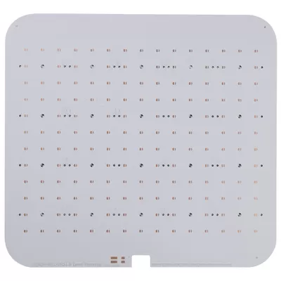
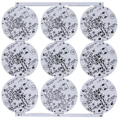
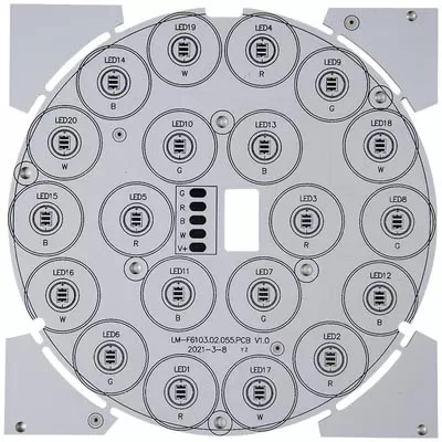
Kingford provides Plant lamp PCB services. This is a PCBA one-stop assembly factory with senior indu...
We are a professional PCBA one-stop assembly factory, Kingford supports Aluminum FR4 PCB business, w...
We support Emergency light PCB business,Kingford is a professional one-stop PCBA service factory, we...
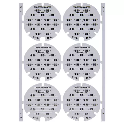
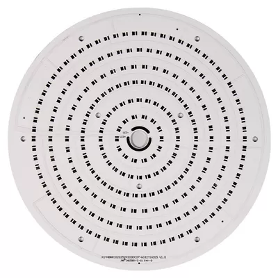
Kingford supports 12W SMD 2835 LED PCB business, we are a professional PCBA one-stop assembly factor...
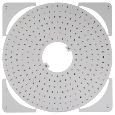
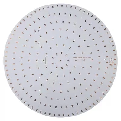
Because the PCB LED light combines excellent energy efficiency, low cost and maximum design flexibil...
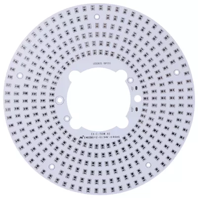
We provide 12W 18W 24W 100W LED PCB services. Kingford is your one stop turnkey PCB assembly factory...
