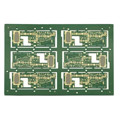
High TG High Frequency Rogers 5880 PCB
Name: High TG High Frequency Rogers 5880 PCB
Substrate: FR4
Copper Thickness: 1 oz
Plate thickness: 1.6mm
minute. Hole size: 0.1mm
minute. Line width: 0.1mm
minute. Line spacing: 0.1mm
Surface Treatment: Immersion Gold
Board size: customized
Silkscreen: White/Black
Solder Mask: Green
Impedance Control Tolerance: 5%
PCB Standard: IPC-A-610 D
Certification: ISO-9001, ISO-1004, ROHS
Material: FR4 CEM1 CEM3 High TG
Minimum thickness: 10 microns
Layers: 1-28
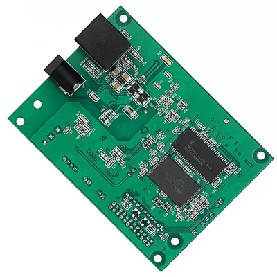
TG180, TG170 communication PCB manufacturing
Name: High Tg cell phone manufacturing electronic pcb
Type: communication pcba
Copper Thickness: 2 oz
Product name: PCBA board assembly
Laminate: FR-4, halogen free, high TG, etc.
Surface treatment: OSP, HASL, Immersion Gold, Immersion Tin, etc.
Plate thickness: 0.3-3.5mm
Solder mask: green, black, blue, red, white, etc.
Blind and buried vias: yes
Independent control tolerance: ±10%
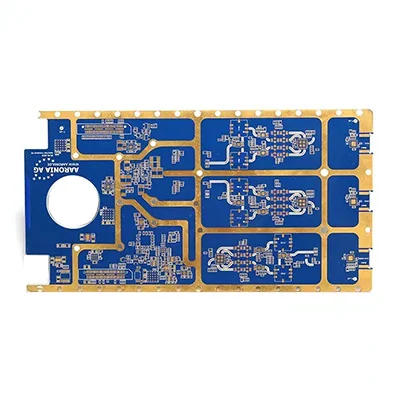
High Tg Single Sided Rogers 4003 pcb
Name: High Tg Single Sided Rogers 4003 pcb
Type: High Frequency Circuit Board
Substrate: Rogers/Taconic/Aron
Copper Thickness: 1 oz
Plate thickness: 1.6mm
minute. Hole size: 0.2mm
minute. Line width: 3 million
minute. Line spacing: 3 million
Board size: 300*600mm, or can be customized
Product Name: High Frequency PCB Board
Layers: 1~20 layers
Testing Service: 100% AOI Testing
Certificate: ISO9001/Iso14001/CE/ROHS
Application: Electronics
High Tg Board High Frequency Rogers 5880 PCB
Name: High Tg Board High Frequency Rogers 5880 PCB
Substrate: FR-4
Copper Thickness: 1 oz
Plate Thickness: 1.6mm, 1.6mm
minute. Hole size: 0.1mm
minute. Line width: 3 million
minute. Line spacing: 3 million
Surface treatment: spray tin lead-free, spray tin lead-free
Board Size: Green Soldermask, White Silkscreen
Minimum aperture: 0.25mm
Minimum line spacing: 0.003"
Color: Green or as your request
Material: FR-4
Layers: 2 layers
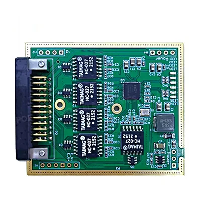
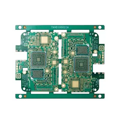
FR4 High TG Multilayer HDI PCB
Name: FR4 High TG Multilayer HDI PCB
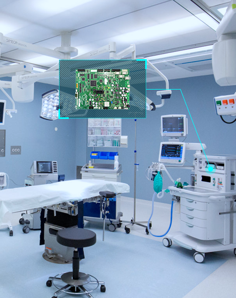
Type: Medical PCBA, PCB Assembly/PCBA
Copper Thickness: 1 oz, 0.5-4 oz, regular 1 oz
Product Name: Printed Circuit Board
Material: FR4/Aluminum/Ceramic CEM1 etc.
Layers: 1-60 layers
Shapes: Rectangle, Circle, Slot, Cutout, Complex, Irregular or Custom.
Plate thickness: 0.2-4mm, conventional 1.6mm
Solder Mask: White.Black.Yellow.Green.Red.Blue or custom.
Name: Fr4 High Tg Multilayer PCB
Model: customized
Substrate: FR4, FR1-4, FR4, FR1-4
Copper Thickness: 0.5oz, 1oz, 2oz, 3oz,4oz, 0.5oz, 1oz, 2oz, 3oz,4oz
Thickness: 0.6MM, 0.4mm-3.2mm, 0.6MM, 0.4mm-3.2mm
Surface treatment: lead-free spray tin, spray tin lead-free
Layers: 1-58 layers
Certificate: ISO9001/RoHS/CE
Solder mask color: green, white
Name: FR4 TG 180 PCB
Base material: FR4, aluminum
Copper Thickness: 0.5-4OZ / 1 Oz / 2Oz or customized
Plate thickness: 0.2~6mm
minute. Hole size: 0.15mm
minute. Line width: 0.015mm
minute. Line spacing: 0.015mm
Surface treatment: tin spray, immersion gold, flash gold, silver plating, OSP
Application: Industrial Control, Medical, Security, IoT Gateway, Internet
Solder mask color: green, red, black (according to your requirements)
Silk screen color: white, black (according to your request)
Layers: 1-64
Certificate: RoHS/ISO9001/TS16949/ISO14001/ISO13485
Packaging: vacuum, anti-static, ESD
8L Multilayer HDI High Tg 180 PCB
Name: 8L Multilayer HDI High Tg 180 pcb
Copper Thickness: 1 oz
Plate Thickness: 1.6mm, 1.6mm
minute. Hole size: 0.1mm
minute. Line width: 3 million
minute. Line spacing: 3 million
Surface treatment: spray tin lead-free, spray tin lead-free
Minimum line spacing: 0.003"
Color: Green or as your request
Material: FR-4
Layers: 2 layers
Packing: vacuum packing
- PCB Manufacturing Equipment
- PCB manufacturing capability

PCB Drilling machine

PCB pattern plating line

PCB solder mask expose machine

PCB pattern expose machine

Strip film etching line

Solder mask screen silk print machine

Solder mask scrubbing line
")
PCB Flying Probe Test (FPT)

Fully automatic exposure machine
| Standard PCB Production Capability | |
| Feature | Capability |
| Quality Grade | Standard IPC 2 |
| Number of Layers | 1 - 32layers |
| Order Quantity | 1pcs - 10,000,000 pcs |
| Build Time | 2days - 5weeks (Expedited Service) |
| Material | FR-4 Standard Tg 150°C, FR4-High Tg 170°C, FR4-High-Tg 180°C, FR4-Halogen-free, FR4-Halogen-free & High-Tg |
| Board Size | Min 6*6mm | Max 600*700mm |
| Board size tolerance | ±0.1mm - ±0.3mm |
| Board Thickness | 0.4mm - 3.2mm |
| Board Thickness Tolerance | ±0.1mm - ±10% |
| Copper Weight | 0.5oz - 6.0oz |
| Inner Layer Copper Weight | 0.5oz - 2.0oz |
| Copper Thickness Tolerance | +0μm +20μm |
| Min Tracing/Spacing | 3mil/3mil |
| Solder Mask Sides | As per the file |
| Solder Mask Color | Green, White, Blue, Black, Red, Yellow |
| Silkscreen Sides | As per the file |
| Silkscreen Color | White, Blue, Black, Red, Yellow |
| Surface Finish | HASL - Hot Air Solder Leveling |
| Lead Free HASL - RoHS | |
| ENIG - Electroless Nickle/Immersion Gold - RoHS | |
| ENEPIG - Electroless Nickel Electroless Palladium Immersion Gold - RoHS | |
| Immersion Silver - RoHS | |
| Immersion Tin - RoHS | |
| OSP -Organic Solderability Preservatives - RoHS | |
| Min Annular Ring | 3mil |
| Min Drilling Hole Diameter | 6mil, 4mil-laser drill |
| Min Width of Cutout (NPTH) | 0.8mm |
| NPTH Hole Size Tolerance | ±.002" (±0.05mm) |
| Min Width of Slot Hole (PTH) | 0.6mm |
| PTH Hole Size Tolerance | ±.003" (±0.08mm) - ±4mil |
| Surface/Hole Plating Thickness | 20μm - 30μm |
| SM Tolerance (LPI) | .003" (0.075mm) |
| Aspect Ratio | 1.10 (hole size: board thickness) |
| Test | 10V - 250V, flying probe or testing fixture |
| Impedance tolerance | ±5% - ±10% |
| SMD Pitch | 0.2mm(8mil) |
| BGA Pitch | 0.2mm(8mil) |
| Chamfer of Gold Fingers | 20, 30, 45, 60 |
| Other Techniques | Gold fingers |
| Blind and Buried Holes | |
| peelable solder mask | |
| Edge plating | |
| Carbon Mask | |
| Kapton tape | |
| Countersink/counterbore hole | |
| Half-cut/Castellated hole | |
| Press fit hole | |
| Via tented/covered with resin | |
| Via plugged/filled with resin | |
| Via in pad | |
| Electrical Test | |

High-standard confidentiality measures, signing confidentiality agreements, and all documents exporting must be approved to ensure that 100% of documents are not leaked.

we provide 24-hour service and support, you will receive a reply to your question within 2 hours and a quotation within 24 hours.

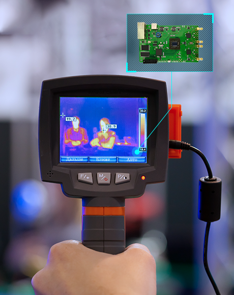
We can provide you with high frequency, high TG, high CTI, buried blind via, aluminum based PCB manufacturing, the quality is fully compliant with IPC 610-D standard, testing and quality assurance

With more than 20 years of industry experience, technology and production capacity are constantly increasing, and we can provide one-stop services from standard PCB to HDI PCB, high frequency and high...

Kingford has stable material suppliers with ten years of cooperation, such as Shengyi Technology, ITEQ, ROGERS, AGC, DUPONT, Doosan, Mitsubishi, etc.
RT/duroid 5880 PTFE composite is suitable for processing in conventional welding and electroplating....
WHAT IS PCB TGWhen the temperature gets high enough, the PCB substrate that consists of glass fiber ...
Excellent high frequency performance of Rogers 4003 materialRogers sheet RO4000 PCB material family ...
What is Rogers 5880?Rogers RT/duroid 5880 high frequency laminate is a PTFE composite reinforced wit...
Tg refers to the glass transition temperature. Since the flammability of printed circuit boards (PCB...
Tg refers to the glass transition temperature. Since the flammability of printed circuit boards (PCB...