


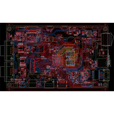
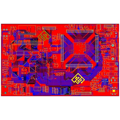
Communication high-speed signal PCBA design
Name: Communication high-speed signal PCBA design
Plate: TG170 /TG180, F4BM, FR4, FR1-4, etc.
Designable layers: 1-32 layers
Minimum line width and line spacing: 3mil
Minimum laser aperture: 4mil
Minimum mechanical aperture: 8mil
Copper foil thickness: 18-175цm (standard: 18цm35цm70цm)
Peel strength: 1.25N/mm
Minimum punching hole diameter: single side: 0.9mm/35mil
Minimum hole diameter: 0.25mm/10mil
Aperture tolerance: ≤φ0.8mm±0.05mm
Hole tolerance: ±0.05mm
Hole wall copper thickness: double-sided/multi-layer: ≥2um/0.8mil
Hole resistance: double-sided/multi-layer: ≤300цΩ
Minimum line width: 0.127mm/5mil
Minimum pitch: 0.127mm/5mil
Screen printing color: black, white, red, green, etc.
Surface treatment: lead/lead-free tin spray, ENIG, silver, OSP
Service: Provide OEM service
Certificate: ISO9001.ROSH.UL
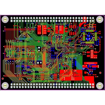
Arbitrary Interconnect HDI PCBA Design
Name: Arbitrary Interconnect HDI PCBA Design
Plate: TG170 /TG180, F4BM, FR4, FR1-4, etc.
Designable layers: 1-32 layers
Minimum line width and line spacing: 3mil
Minimum laser aperture: 4mil
Minimum mechanical aperture: 8mil
Copper foil thickness: 18-175цm (standard: 18цm35цm70цm)
Peel strength: 1.25N/mm
Minimum punching hole diameter: single side: 0.9mm/35mil
Minimum hole diameter: 0.25mm/10mil
Aperture tolerance: ≤φ0.8mm±0.05mm
Hole tolerance: ±0.05mm
Hole wall copper thickness: double-sided/multi-layer: ≥2um/0.8mil
Hole resistance: double-sided/multi-layer: ≤300цΩ
Minimum line width: 0.127mm/5mil
Minimum pitch: 0.127mm/5mil
Screen printing color: black, white, red, green, etc.
Surface treatment: lead/lead-free tin spray, ENIG, silver, OSP
Service: Provide OEM service
Certificate: ISO9001.ROSH.UL
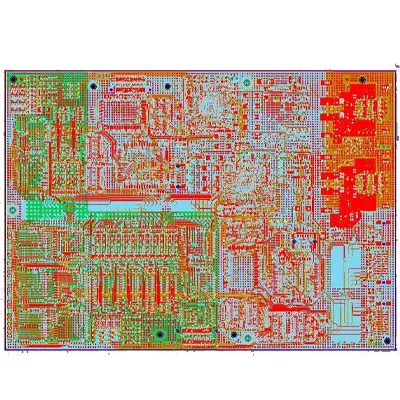
10-layer second-order HDI PCBA design
Name: 10-layer second-order HDI PCBA design
Plate: TG170 /TG180, F4BM, FR4, FR1-4, etc.
Designable layers: 1-32 layers
Minimum line width and line spacing: 3mil
Minimum laser aperture: 4mil
Minimum mechanical aperture: 8mil
Copper foil thickness: 18-175цm (standard: 18цm35цm70цm)
Peel strength: 1.25N/mm
Minimum punching hole diameter: single side: 0.9mm/35mil
Minimum hole diameter: 0.25mm/10mil
Aperture tolerance: ≤φ0.8mm±0.05mm
Hole tolerance: ±0.05mm
Hole wall copper thickness: double-sided/multi-layer: ≥2um/0.8mil
Hole resistance: double-sided/multi-layer: ≤300цΩ
Minimum line width: 0.127mm/5mil
Minimum pitch: 0.127mm/5mil
Screen printing color: black, white, red, green, etc.
Surface treatment: lead/lead-free tin spray, ENIG, silver, OSP
Service: Provide OEM service
Certificate: ISO9001.ROSH.UL
16-layer two-stage high-precision PCB design
Name: 16-layer two-stage high-precision PCB design
Plate: TG170 /TG180, F4BM, FR4, FR1-4, etc.
Designable layers: 1-32 layers
Minimum line width and line spacing: 3mil
Minimum laser aperture: 4mil
Minimum mechanical aperture: 8mil
Copper foil thickness: 18-175цm (standard: 18цm35цm70цm)
Peel strength: 1.25N/mm
Minimum punching hole diameter: single side: 0.9mm/35mil
Minimum hole diameter: 0.25mm/10mil
Aperture tolerance: ≤φ0.8mm±0.05mm
Hole tolerance: ±0.05mm
Hole wall copper thickness: double-sided/multi-layer: ≥2um/0.8mil
Hole resistance: double-sided/multi-layer: ≤300цΩ
Minimum line width: 0.127mm/5mil
Minimum pitch: 0.127mm/5mil
Screen printing color: black, white, red, green, etc.
Surface treatment: lead/lead-free tin spray, ENIG, silver, OSP
Service: Provide OEM service
Certificate: ISO9001.ROSH.UL
8-layer second-order HDI PCBA design
Name: 8-layer second-order HDI PCBA design
Plate: TG170 /TG180, F4BM, FR4, FR1-4, etc.
Designable layers: 1-32 layers
Minimum line width and line spacing: 3mil
Minimum laser aperture: 4mil
Minimum mechanical aperture: 8mil
Copper foil thickness: 18-175цm (standard: 18цm35цm70цm)
Peel strength: 1.25N/mm
Minimum punching hole diameter: single side: 0.9mm/35mil
Minimum hole diameter: 0.25mm/10mil
Aperture tolerance: ≤φ0.8mm±0.05mm
Hole tolerance: ±0.05mm
Hole wall copper thickness: double-sided/multi-layer: ≥2um/0.8mil
Hole resistance: double-sided/multi-layer: ≤300цΩ
Minimum line width: 0.127mm/5mil
Minimum pitch: 0.127mm/5mil
Screen printing color: black, white, red, green, etc.
Surface treatment: lead/lead-free tin spray, ENIG, silver, OSP
Service: Provide OEM service
Certificate: ISO9001.ROSH.UL
Six-layer HDI PCBA design and production
Name: TG180 High Density Interconnector PCBA Design
Plate: TG170 /TG180, F4BM, FR4, FR1-4, etc.
Designable layers: 1-32 layers
Minimum line width and line spacing: 3mil
Minimum laser aperture: 4mil
Minimum mechanical aperture: 8mil
Copper foil thickness: 18-175цm (standard: 18цm35цm70цm)
Peel strength: 1.25N/mm
Minimum punching hole diameter: single side: 0.9mm/35mil
Minimum hole diameter: 0.25mm/10mil
Aperture tolerance: ≤φ0.8mm±0.05mm
Hole tolerance: ±0.05mm
Hole wall copper thickness: double-sided/multi-layer: ≥2um/0.8mil
Hole resistance: double-sided/multi-layer: ≤300цΩ
Minimum line width: 0.127mm/5mil
Minimum pitch: 0.127mm/5mil
Screen printing color: black, white, red, green, etc.
Surface treatment: lead/lead-free tin spray, ENIG, silver, OSP
Service: Provide OEM service
Certificate: ISO9001.ROSH.UL
Automation Equipment HDI PCBA Design
Name: Automation Equipment HDI PCBA Design
Sheet: IT180, F4BM, FR4, FR1-4, etc.
Designable layers: 1-32 layers
Minimum line width and line spacing: 3mil
Minimum laser aperture: 4mil
Minimum mechanical aperture: 8mil
Copper foil thickness: 18-175цm (standard: 18цm35цm70цm)
Peel strength: 1.25N/mm
Minimum punching hole diameter: single side: 0.9mm/35mil
Minimum hole diameter: 0.25mm/10mil
Aperture tolerance: ≤φ0.8mm±0.05mm
Hole tolerance: ±0.05mm
Hole wall copper thickness: double-sided/multi-layer: ≥2um/0.8mil
Hole resistance: double-sided/multi-layer: ≤300цΩ
Minimum line width: 0.127mm/5mil
Minimum pitch: 0.127mm/5mil
Surface treatment: rosin spray tin electric gold, anti-oxidation, chemical gold, carbon oil
Service: Provide OEM service
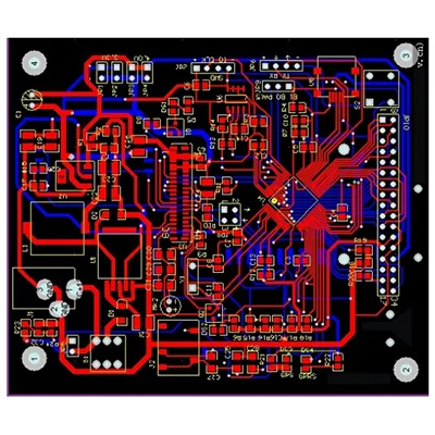
4-layer HDI switch circuit board design
Name: 4-layer HDI switch circuit board design
Sheet: IT180, F4BM, FR4, FR1-4, etc.
Designable layers: 1-32 layers
Minimum line width and line spacing: 3mil
Minimum laser aperture: 4mil
Minimum mechanical aperture: 8mil
Copper foil thickness: 18-175цm (standard: 18цm35цm70цm)
Peel strength: 1.25N/mm
Minimum punching hole diameter: single side: 0.9mm/35mil
Minimum hole diameter: 0.25mm/10mil
Aperture tolerance: ≤φ0.8mm±0.05mm
Hole tolerance: ±0.05mm
Hole wall copper thickness: double-sided/multi-layer: ≥2um/0.8mil
Hole resistance: double-sided/multi-layer: ≤300цΩ
Minimum line width: 0.127mm/5mil
Minimum pitch: 0.127mm/5mil
Surface treatment: rosin spray tin electric gold, anti-oxidation, chemical gold, carbon oil
Service: Provide OEM service
- PCB Design Capabilities
| PCB Design&Layout Capabilities | |||
| Min.trace width: | 2.5mil | Min.trace spacing | 2.5mil |
| Min.Vias: | 6mil(4mil laser drilling) | Max.layer | 48L |
| Min.BGA spacing | 0.35mm | Max.BGA Pin | 3600pin |
| Max.high-speed signal | 40 GBPS | Fastest delivery time | 6 Hours/ Item |
| HDI Highest layer | 22 L | HDI Highest layer | 14 L any layer HDI |
| PCB Design&Layout lead time | |||
| Number of pins on the board | 0-1000 | Design lead time (working days) | 3-5 days |
| 2000-3000 | 5-8 days | ||
| 4000-5000 | 8-12 days | ||
| 6000-7000 | 12-15 days | ||
| 8000-9000 | 15-18 days | ||
| 10000-12000 | 18-20 days | ||
| 13000-15000 | 20-22 days | ||
| 16000-18000 | 22-25 days | ||
| 18000-20000 | 25-30 days | ||
| Ultimate delivery capacity | 10000Pin/7 days | ||
| PS: The above delivery date is the regular delivery date, and the accurate design delivery date needs to be comprehensively evaluated according to the number of components, difficulty, layers and other factors of the circuit board! | |||

System advanced training, from beginners to experts, there are various technical special trainings every week.

Self-developed tool software and strict quality control system to ensure a successful one-time board opening

Parallel design to shorten lead time, conventional can shorten PCB design time by 50%

The maximum design scale is 90000pin, which can provide HDI/Any layer PCB design, 3D PCB design, RF design, 56G high-speed design, etc.

With a strict quality system process and a strict review system, we have zero error rate quality requirements for PCB design.

PCB design team with an average of more than 12 years of work experience, with complete design software, such as Cadence Allegro\ORCAD, Mentor WG\PADS, etc.

High-standard confidentiality measures, signing confidentiality agreements, and all documents exporting must be approved to ensure that 100% of documents are not leaked.

we provide 24-hour service and support, you will receive a reply to your question within 2 hours and a quotation within 24 hours.
High Speed Digital Design FundamentalsSo what is high-speed board design? High-speed design specific...
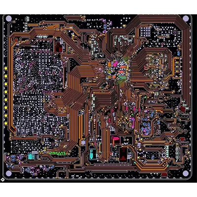
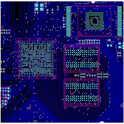
Any Layer HDI PCB: This is the most complex HDI PCB design structure, where all layers are high-dens...
HDI PCB (2+N+2): This is a moderately complex HDI PCB layout design structure that contains 2 or mor...
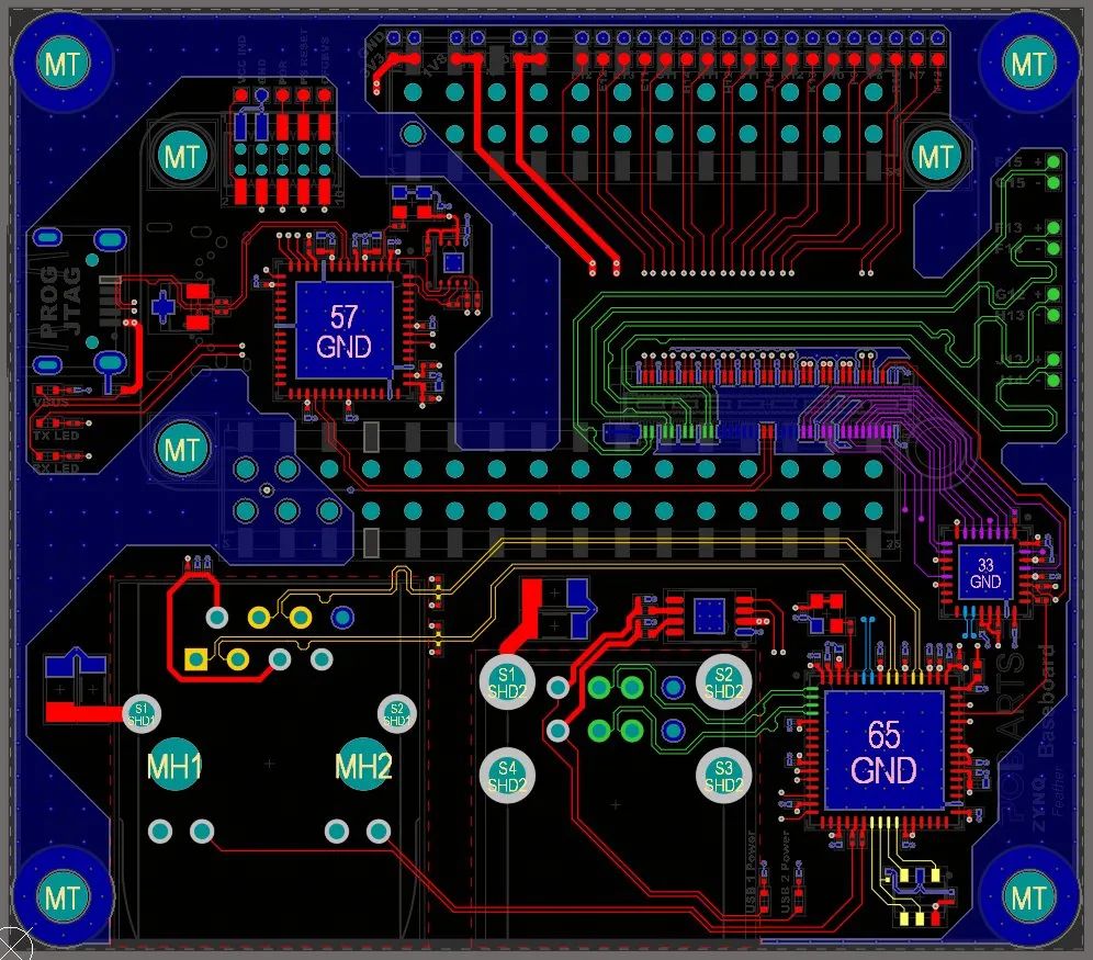
A 16-layer stack has 16 layers of routing and is typically used for high-density designs. In EDA app...
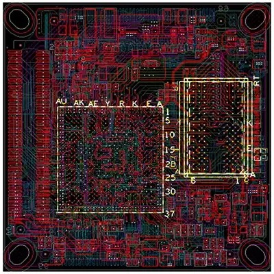
For BGAs with smaller ball pitch and higher I/O countIncrease routing density in complex designsShee...
This is a 6-layer HDI rigid flex PCB with blind and buried vias. Made of the most common rigid insul...


As products are miniaturized, many designs push the physical limits of PCB manufacturability. In this context, the importance of DFM inspection is increasing.
Multilayer PCB Design FAQ
Some DFM problems include: problems due to copper/solder mask debris on the plane, problems due to no gap pads on the plane, problems due to insufficient annular rings, problems due to copper being too close to the edge of the board.
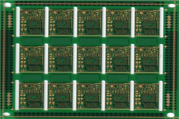
HDI PCB Design High Density Interconnector PCB Design. Circuit boards with higher wiring density per unit area compared to traditional circuit boards are called HDI PCBs.
