

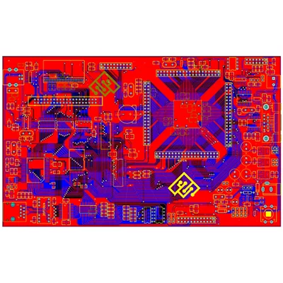
Automation Equipment HDI PCBA Design
Name: Automation Equipment HDI PCBA Design
Sheet: IT180, F4BM, FR4, FR1-4, etc.
Designable layers: 1-32 layers
Minimum line width and line spacing: 3mil
Minimum laser aperture: 4mil
Minimum mechanical aperture: 8mil
Copper foil thickness: 18-175цm (standard: 18цm35цm70цm)
Peel strength: 1.25N/mm
Minimum punching hole diameter: single side: 0.9mm/35mil
Minimum hole diameter: 0.25mm/10mil
Aperture tolerance: ≤φ0.8mm±0.05mm
Hole tolerance: ±0.05mm
Hole wall copper thickness: double-sided/multi-layer: ≥2um/0.8mil
Hole resistance: double-sided/multi-layer: ≤300цΩ
Minimum line width: 0.127mm/5mil
Minimum pitch: 0.127mm/5mil
Surface treatment: rosin spray tin electric gold, anti-oxidation, chemical gold, carbon oil
Service: Provide OEM service
What are the advantages of HDI PCB?
Extraordinary versatility: HDI boards are ideal when weight, space, reliability and performance are the main concerns.
Compact design: The combination of blind, buried and micro vias reduces board space requirements.
Better Signal Integrity: HDI utilizes via-in-pad and blind via technology. This helps keep components close to each other, reducing signal path lengths. HDI technology removes through-hole stubs, thus reducing signal reflections, thereby improving signal quality. Therefore, it significantly improves signal integrity due to shorter signal paths.
High reliability: The implementation of stacked vias makes these boards a super barrier against extreme environmental conditions.
Cost-effective: The functionality of a standard 8-layer through-hole board (standard PCB) can be reduced to a 6-layer HDI board without compromising the quality.
Name: Automation Equipment HDI PCBA Design
Sheet: IT180, F4BM, FR4, FR1-4, etc.
Designable layers: 1-32 layers
Minimum line width and line spacing: 3mil
Minimum laser aperture: 4mil
Minimum mechanical aperture: 8mil
Copper foil thickness: 18-175цm (standard: 18цm35цm70цm)
Peel strength: 1.25N/mm
Minimum punching hole diameter: single side: 0.9mm/35mil
Minimum hole diameter: 0.25mm/10mil
Aperture tolerance: ≤φ0.8mm±0.05mm
Hole tolerance: ±0.05mm
Hole wall copper thickness: double-sided/multi-layer: ≥2um/0.8mil
Hole resistance: double-sided/multi-layer: ≤300цΩ
Minimum line width: 0.127mm/5mil
Minimum pitch: 0.127mm/5mil
Surface treatment: rosin spray tin electric gold, anti-oxidation, chemical gold, carbon oil
Service: Provide OEM service
