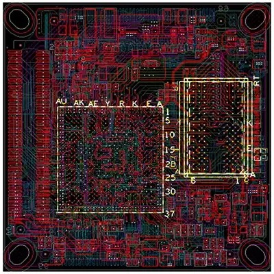
Communication high-speed signal PCBA design
Name: Communication high-speed signal PCBA design
Plate: TG170 /TG180, F4BM, FR4, FR1-4, etc.
Designable layers: 1-32 layers
Minimum line width and line spacing: 3mil
Minimum laser aperture: 4mil
Minimum mechanical aperture: 8mil
Copper foil thickness: 18-175цm (standard: 18цm35цm70цm)
Peel strength: 1.25N/mm
Minimum punching hole diameter: single side: 0.9mm/35mil
Minimum hole diameter: 0.25mm/10mil
Aperture tolerance: ≤φ0.8mm±0.05mm
Hole tolerance: ±0.05mm
Hole wall copper thickness: double-sided/multi-layer: ≥2um/0.8mil
Hole resistance: double-sided/multi-layer: ≤300цΩ
Minimum line width: 0.127mm/5mil
Minimum pitch: 0.127mm/5mil
Screen printing color: black, white, red, green, etc.
Surface treatment: lead/lead-free tin spray, ENIG, silver, OSP
Service: Provide OEM service
Certificate: ISO9001.ROSH.UL
High Speed Digital Design Fundamentals
So what is high-speed board design? High-speed design specifically refers to systems that use high-speed digital signals to transfer data between components. The line between high-speed digital designs and simple circuit boards with slower digital protocols is blurred. A common metric used to denote a particular system as "high speed" is the edge rate (or rise time) of the digital signals used in the system. Most digital designs use both high-speed (fast edge rate) and low-speed (slow edge rate) digital protocols. In today's era of embedded computing and the Internet of Things, most high-speed circuit boards have an RF front-end for wireless communication and networking.
All PCB stack-ups include a set of layers dedicated to high-speed signal, power, and ground planes, and the following points need to be considered when assigning layers in the stack-up:
Board size and net count: How big is the board and how many nets need to be routed in the PCB layout. A physically larger board may have enough space for you to route the entire PCB layout without using multiple signal layers.
Routing Density: With a high number of nets and board size constrained by a small area, you may not have enough room to route around the surface layers. So when the traces are closer together, you will need more internal signal layers. Using a smaller board size can force higher routing density.
Number of interfaces: Sometimes routing only one or two interfaces per layer is a good strategy, depending on the width of the bus (serial vs. parallel) and board size. Keeping all signals in a high-speed digital interface on the same layer ensures that all signals see consistent impedance and skew.
Low-speed and RF signals: Will there be low-speed digital or RF signals in your digital design? If so, these may take up surface space available for high-speed buses or components, and may require additional internal layers.
Power Integrity: One of the cornerstones of power integrity is the use of large power and ground planes for every voltage level required by a large IC. These should be placed on adjacent layers to help ensure that there is high plane capacitance to support a stable power supply with decoupling capacitors.
Name: Communication high-speed signal PCBA design
Plate: TG170 /TG180, F4BM, FR4, FR1-4, etc.
Designable layers: 1-32 layers
Minimum line width and line spacing: 3mil
Minimum laser aperture: 4mil
Minimum mechanical aperture: 8mil
Copper foil thickness: 18-175цm (standard: 18цm35цm70цm)
Peel strength: 1.25N/mm
Minimum punching hole diameter: single side: 0.9mm/35mil
Minimum hole diameter: 0.25mm/10mil
Aperture tolerance: ≤φ0.8mm±0.05mm
Hole tolerance: ±0.05mm
Hole wall copper thickness: double-sided/multi-layer: ≥2um/0.8mil
Hole resistance: double-sided/multi-layer: ≤300цΩ
Minimum line width: 0.127mm/5mil
Minimum pitch: 0.127mm/5mil
Screen printing color: black, white, red, green, etc.
Surface treatment: lead/lead-free tin spray, ENIG, silver, OSP
Service: Provide OEM service
Certificate: ISO9001.ROSH.UL


