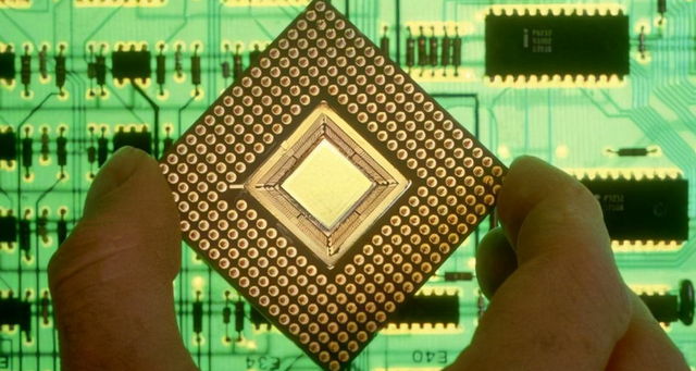
High Frequency High Speed PCB Design
Name: High Frequency High Speed PCB Design
Plate: TG170 /TG180, F4BM, FR4, FR1-4, etc.
Designable layers: 1-32 layers
Minimum line width and line spacing: 3mil
Minimum laser aperture: 4mil
Minimum mechanical aperture: 8mil
Copper foil thickness: 18-175цm (standard: 18цm35цm70цm)
Peel strength: 1.25N/mm
Minimum punching hole diameter: single side: 0.9mm/35mil
Minimum hole diameter: 0.25mm/10mil
Aperture tolerance: ≤φ0.8mm±0.05mm
Hole tolerance: ±0.05mm
Hole wall copper thickness: double-sided/multi-layer: ≥2um/0.8mil
Hole resistance: double-sided/multi-layer: ≤300цΩ
Minimum line width: 0.127mm/5mil
Minimum pitch: 0.127mm/5mil
Screen printing color: black, white, red, green, etc.
Surface treatment: lead/lead-free tin spray, ENIG, silver, OSP
Service: Provide OEM service
Certificate: ISO9001.ROSH.UL
artificial intelligence circuit board design
Name: artificial intelligence circuit board design
Plate: TG170 /TG180, F4BM, FR4, FR1-4, etc.
Designable layers: 1-32 layers
Minimum line width and line spacing: 3mil
Minimum laser aperture: 4mil
Minimum mechanical aperture: 8mil
Copper foil thickness: 18-175цm (standard: 18цm35цm70цm)
Peel strength: 1.25N/mm
Minimum punching hole diameter: single side: 0.9mm/35mil
Minimum hole diameter: 0.25mm/10mil
Aperture tolerance: ≤φ0.8mm±0.05mm
Hole tolerance: ±0.05mm
Hole wall copper thickness: double-sided/multi-layer: ≥2um/0.8mil
Hole resistance: double-sided/multi-layer: ≤300цΩ
Minimum line width: 0.127mm/5mil
Minimum pitch: 0.127mm/5mil
Screen printing color: black, white, red, green, etc.
Surface treatment: lead/lead-free tin spray, ENIG, silver, OSP
Service: Provide OEM service
Certificate: ISO9001.ROSH.UL
Communication terminal circuit board design
Name: Communication terminal circuit board design
Plate: TG170 /TG180, F4BM, FR4, FR1-4, etc.
Designable layers: 1-32 layers
Minimum line width and line spacing: 3mil
Minimum laser aperture: 4mil
Minimum mechanical aperture: 8mil
Copper foil thickness: 18-175цm (standard: 18цm35цm70цm)
Peel strength: 1.25N/mm
Minimum punching hole diameter: single side: 0.9mm/35mil
Minimum hole diameter: 0.25mm/10mil
Aperture tolerance: ≤φ0.8mm±0.05mm
Hole tolerance: ±0.05mm
Hole wall copper thickness: double-sided/multi-layer: ≥2um/0.8mil
Hole resistance: double-sided/multi-layer: ≤300цΩ
Minimum line width: 0.127mm/5mil
Minimum pitch: 0.127mm/5mil
Screen printing color: black, white, red, green, etc.
Surface treatment: lead/lead-free tin spray, ENIG, silver, OSP
Service: Provide OEM service
Certificate: ISO9001.ROSH.UL
High Speed Server Backplane PCB Design
Name: High Speed Server Backplane PCB Design
Plate: TG170 /TG180, F4BM, FR4, FR1-4, etc.
Designable layers: 1-32 layers
Minimum line width and line spacing: 3mil
Minimum laser aperture: 4mil
Minimum mechanical aperture: 8mil
Copper foil thickness: 18-175цm (standard: 18цm35цm70цm)
Peel strength: 1.25N/mm
Minimum punching hole diameter: single side: 0.9mm/35mil
Minimum hole diameter: 0.25mm/10mil
Aperture tolerance: ≤φ0.8mm±0.05mm
Hole tolerance: ±0.05mm
Hole wall copper thickness: double-sided/multi-layer: ≥2um/0.8mil
Hole resistance: double-sided/multi-layer: ≤300цΩ
Minimum line width: 0.127mm/5mil
Minimum pitch: 0.127mm/5mil
Screen printing color: black, white, red, green, etc.
Surface treatment: lead/lead-free tin spray, ENIG, silver, OSP
Service: Provide OEM service
Certificate: ISO9001.ROSH.UL
High-speed and high-density PCBA design
Name: High-speed and high-density PCBA design
Plate: TG170 /TG180, F4BM, FR4, FR1-4, etc.
Designable layers: 1-32 layers
Minimum line width and line spacing: 3mil
Minimum laser aperture: 4mil
Minimum mechanical aperture: 8mil
Copper foil thickness: 18-175цm (standard: 18цm35цm70цm)
Peel strength: 1.25N/mm
Minimum punching hole diameter: single side: 0.9mm/35mil
Minimum hole diameter: 0.25mm/10mil
Aperture tolerance: ≤φ0.8mm±0.05mm
Hole tolerance: ±0.05mm
Hole wall copper thickness: double-sided/multi-layer: ≥2um/0.8mil
Hole resistance: double-sided/multi-layer: ≤300цΩ
Minimum line width: 0.127mm/5mil
Minimum pitch: 0.127mm/5mil
Screen printing color: black, white, red, green, etc.
Surface treatment: lead/lead-free tin spray, ENIG, silver, OSP
Service: Provide OEM service
Certificate: ISO9001.ROSH.UL
12-layer automotive high-speed backplane design
Name: 12-layer automotive high-speed backplane design
Plate: TG170 /TG180, F4BM, FR4, FR1-4, etc.
Designable layers: 1-32 layers
Minimum line width and line spacing: 3mil
Minimum laser aperture: 4mil
Minimum mechanical aperture: 8mil
Copper foil thickness: 18-175цm (standard: 18цm35цm70цm)
Peel strength: 1.25N/mm
Minimum punching hole diameter: single side: 0.9mm/35mil
Minimum hole diameter: 0.25mm/10mil
Aperture tolerance: ≤φ0.8mm±0.05mm
Hole tolerance: ±0.05mm
Hole wall copper thickness: double-sided/multi-layer: ≥2um/0.8mil
Hole resistance: double-sided/multi-layer: ≤300цΩ
Minimum line width: 0.127mm/5mil
Minimum pitch: 0.127mm/5mil
Screen printing color: black, white, red, green, etc.
Surface treatment: lead/lead-free tin spray, ENIG, silver, OSP
Service: Provide OEM service
Certificate: ISO9001.ROSH.UL
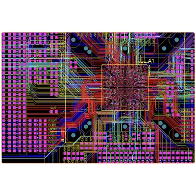
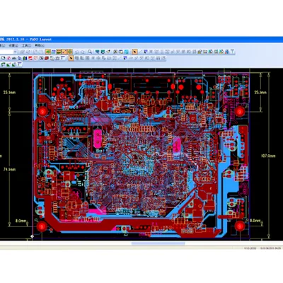
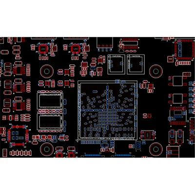
- PCB Design Capabilities
| PCB Design&Layout Capabilities | |||
| Min.trace width: | 2.5mil | Min.trace spacing | 2.5mil |
| Min.Vias: | 6mil(4mil laser drilling) | Max.layer | 48L |
| Min.BGA spacing | 0.35mm | Max.BGA Pin | 3600pin |
| Max.high-speed signal | 40 GBPS | Fastest delivery time | 6 Hours/ Item |
| HDI Highest layer | 22 L | HDI Highest layer | 14 L any layer HDI |
| PCB Design&Layout lead time | |||
| Number of pins on the board | 0-1000 | Design lead time (working days) | 3-5 days |
| 2000-3000 | 5-8 days | ||
| 4000-5000 | 8-12 days | ||
| 6000-7000 | 12-15 days | ||
| 8000-9000 | 15-18 days | ||
| 10000-12000 | 18-20 days | ||
| 13000-15000 | 20-22 days | ||
| 16000-18000 | 22-25 days | ||
| 18000-20000 | 25-30 days | ||
| Ultimate delivery capacity | 10000Pin/7 days | ||
| PS: The above delivery date is the regular delivery date, and the accurate design delivery date needs to be comprehensively evaluated according to the number of components, difficulty, layers and other factors of the circuit board! | |||

System advanced training, from beginners to experts, there are various technical special trainings every week.

Self-developed tool software and strict quality control system to ensure a successful one-time board opening

Parallel design to shorten lead time, conventional can shorten PCB design time by 50%

The maximum design scale is 90000pin, which can provide HDI/Any layer PCB design, 3D PCB design, RF design, 56G high-speed design, etc.

With a strict quality system process and a strict review system, we have zero error rate quality requirements for PCB design.

PCB design team with an average of more than 12 years of work experience, with complete design software, such as Cadence Allegro\ORCAD, Mentor WG\PADS, etc.

High-standard confidentiality measures, signing confidentiality agreements, and all documents exporting must be approved to ensure that 100% of documents are not leaked.

we provide 24-hour service and support, you will receive a reply to your question within 2 hours and a quotation within 24 hours.
The high-frequency hybrid splint includes a base plate, which is folded and positioned on the first ...
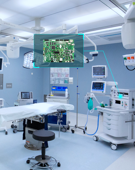
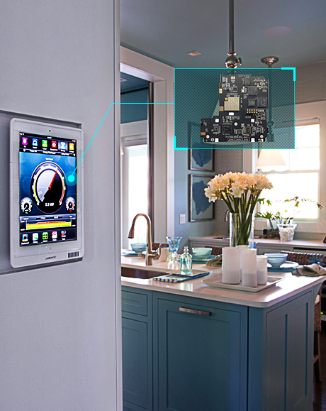
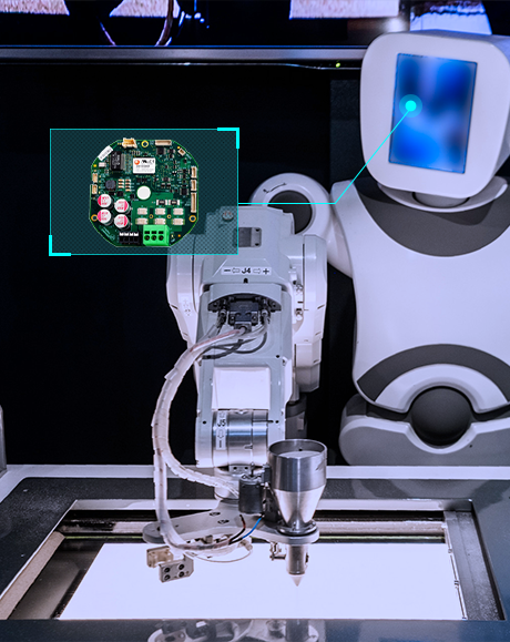
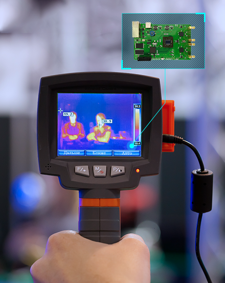
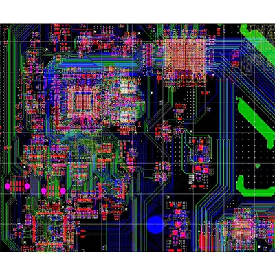
It embellishes every highlight of modern life. Intelligent circuit boards connect circuit informatio...
The high-frequency hybrid splint includes a base plate, which is folded and positioned on the first ...
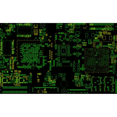
Backplanes are advanced circuit boards that borrow some elements from high-speed design, mechanical ...
What is high speed in PCB?In short, high-speed PCB design is any design where signal integrity begin...
feature Small size provides significant space savings Modular design provides application flexibil...