High Frequency High Speed PCB Design
Name: High Frequency High Speed PCB Design
Plate: TG170 /TG180, F4BM, FR4, FR1-4, etc.
Designable layers: 1-32 layers
Minimum line width and line spacing: 3mil
Minimum laser aperture: 4mil
Minimum mechanical aperture: 8mil
Copper foil thickness: 18-175цm (standard: 18цm35цm70цm)
Peel strength: 1.25N/mm
Minimum punching hole diameter: single side: 0.9mm/35mil
Minimum hole diameter: 0.25mm/10mil
Aperture tolerance: ≤φ0.8mm±0.05mm
Hole tolerance: ±0.05mm
Hole wall copper thickness: double-sided/multi-layer: ≥2um/0.8mil
Hole resistance: double-sided/multi-layer: ≤300цΩ
Minimum line width: 0.127mm/5mil
Minimum pitch: 0.127mm/5mil
Screen printing color: black, white, red, green, etc.
Surface treatment: lead/lead-free tin spray, ENIG, silver, OSP
Service: Provide OEM service
Certificate: ISO9001.ROSH.UL
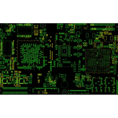
The high-frequency hybrid splint includes a base plate, which is folded and positioned on the first inner wire layer, the first outer wire layer, and the top surface of the solder mask ink layer from top to bottom in order from bottom to top. The second layer of solder resist ink layer, the substrate includes a high-frequency area and an auxiliary area, the auxiliary area is finally fixed, and the inlay in the high-frequency area should be located at a fixed position. The utility model provides a high-frequency hybrid splint, which is divided into two parts: a high-frequency area and an auxiliary area. Provide mechanical support. The utility model discloses that the high-frequency area is independently arranged, and only the high-frequency area is made of high-frequency materials. Under the condition of satisfying high-frequency signals, the use of high-frequency board materials is minimized and the production cost is reduced.High Frequency Hybrid Product Classification Layers: 6 Layers Used Board: ro4350b +FR4 Thickness: 1.6mm Size: 210mm*280mm Surface Treatment: Gold-plated Minimum Aperture: 0.25mm Application: Communication Features: High Frequency Mixed Pressure
Name: High Frequency High Speed PCB Design
Plate: TG170 /TG180, F4BM, FR4, FR1-4, etc.
Designable layers: 1-32 layers
Minimum line width and line spacing: 3mil
Minimum laser aperture: 4mil
Minimum mechanical aperture: 8mil
Copper foil thickness: 18-175цm (standard: 18цm35цm70цm)
Peel strength: 1.25N/mm
Minimum punching hole diameter: single side: 0.9mm/35mil
Minimum hole diameter: 0.25mm/10mil
Aperture tolerance: ≤φ0.8mm±0.05mm
Hole tolerance: ±0.05mm
Hole wall copper thickness: double-sided/multi-layer: ≥2um/0.8mil
Hole resistance: double-sided/multi-layer: ≤300цΩ
Minimum line width: 0.127mm/5mil
Minimum pitch: 0.127mm/5mil
Screen printing color: black, white, red, green, etc.
Surface treatment: lead/lead-free tin spray, ENIG, silver, OSP
Service: Provide OEM service
Certificate: ISO9001.ROSH.UL