

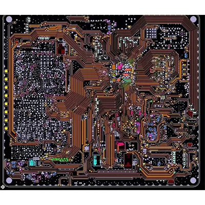
Arbitrary Interconnect HDI PCBA Design
Name: Arbitrary Interconnect HDI PCBA Design
Plate: TG170 /TG180, F4BM, FR4, FR1-4, etc.
Designable layers: 1-32 layers
Minimum line width and line spacing: 3mil
Minimum laser aperture: 4mil
Minimum mechanical aperture: 8mil
Copper foil thickness: 18-175цm (standard: 18цm35цm70цm)
Peel strength: 1.25N/mm
Minimum punching hole diameter: single side: 0.9mm/35mil
Minimum hole diameter: 0.25mm/10mil
Aperture tolerance: ≤φ0.8mm±0.05mm
Hole tolerance: ±0.05mm
Hole wall copper thickness: double-sided/multi-layer: ≥2um/0.8mil
Hole resistance: double-sided/multi-layer: ≤300цΩ
Minimum line width: 0.127mm/5mil
Minimum pitch: 0.127mm/5mil
Screen printing color: black, white, red, green, etc.
Surface treatment: lead/lead-free tin spray, ENIG, silver, OSP
Service: Provide OEM service
Certificate: ISO9001.ROSH.UL
Any Layer HDI PCB: This is the most complex HDI PCB design structure, where all layers are high-density interconnect layers, allowing free interconnection of conductors on any layer of the PCB with the copper-filled stacked microvia structure. This structure provides a reliable interconnect solution for highly complex, high pin-count devices, such as CPU and GPU chips used in handheld and mobile devices, while yielding excellent electrical characteristics.
Name: Arbitrary Interconnect HDI PCBA Design
Plate: TG170 /TG180, F4BM, FR4, FR1-4, etc.
Designable layers: 1-32 layers
Minimum line width and line spacing: 3mil
Minimum laser aperture: 4mil
Minimum mechanical aperture: 8mil
Copper foil thickness: 18-175цm (standard: 18цm35цm70цm)
Peel strength: 1.25N/mm
Minimum punching hole diameter: single side: 0.9mm/35mil
Minimum hole diameter: 0.25mm/10mil
Aperture tolerance: ≤φ0.8mm±0.05mm
Hole tolerance: ±0.05mm
Hole wall copper thickness: double-sided/multi-layer: ≥2um/0.8mil
Hole resistance: double-sided/multi-layer: ≤300цΩ
Minimum line width: 0.127mm/5mil
Minimum pitch: 0.127mm/5mil
Screen printing color: black, white, red, green, etc.
Surface treatment: lead/lead-free tin spray, ENIG, silver, OSP
Service: Provide OEM service
Certificate: ISO9001.ROSH.UL
