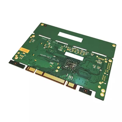
Multilayer Goldfinger Mainboard Control PCB
Name: Multilayer Gold Finger Mainboard Control PCB
Type: Multilayer circuit board
Layers: 6 layers
Substrate: FR4, Aluminum, High Tg FR4
Copper Thickness: 0.5-1 oz
Plate thickness: 0.4-4.0mm
minute. Hole size: 0.15-0.2mm
minute. Line width: 0.1-0.3mm
minute. Line spacing: 0.1-0.3mm
Surface treatment: Immersion gold, spray tin, gold finger
Solder Mask: Green
Applicable to: LED, mobile phone, computer, air conditioner
Certification: ISO-9001, ISO-14001, RoHS
Weight: 0.01-5KG
Application: Electronic Equipment
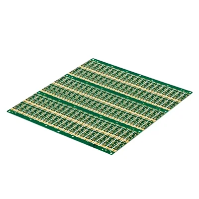
FR4 double-sided gold finger PCB
Name: FR4 double-sided gold finger PCB
Substrate: FR-4 CEM-3 CEM-1
Copper Thickness: 0.5oz-4oz
Plate thickness: 0.4T-4.0T
minute. Hole size: 0.2 million
minute. Line width: 3 million
minute. Line spacing: 3 million
Surface Treatment: OSP/HASL/ENG
Board size: 10*1200mm
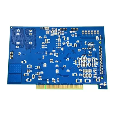
Product name: circuit board
Solder mask color: white black yellow green red blue
Layers: 1-12 layers
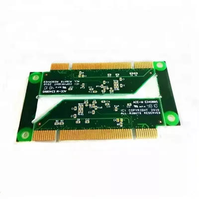
Name: 8-layer Goldfinger PCB
Layers: 8 layers
Substrate: FR-4
Copper Thickness: 2 oz
Plate thickness: 1.6mm
minute. Hole size: 0.3mm
minute. Line width: 0.1mm/4mil
minute. Line spacing: 0.1mm/4mil
Surface Treatment: Immersion Gold
Board size: 168mm*98mm
CCL material: FR-4 RF-35
Profile/Profile: CNC Milling, Milling, Drilling
Jigsaw: one panel, one piece
Blind and buried vias: yes
Special: high frequency coating
Maximum aspect ratio: 8:1
Maximum board size: 600mm*600mm
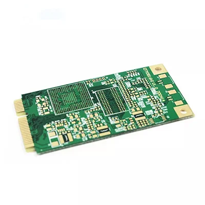
Name: Gold Finger Printed PCB
Substrate: FR-4/High TG
Copper Thickness: 1 oz
Plate thickness: 1.6mm
minute. Hole size: 0.2mm
minute. Line width: 0.1mm/4mil
minute. Line spacing: 0.1mm/4mil
Surface treatment: ENIG
Impedance Control: 50/90/100±10% ohm
TG value: T170
Material flame retardant: 94v0
Standard: IPC-A-610G CLASS II&III
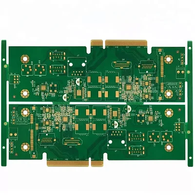
Gold Finger Metal Detector PCB
Name: Gold Finger Metal Detector PCB
Model: Rigid PCB-416
Substrate: FR-4
Copper Thickness: 0.25 oz - 12 oz
Plate thickness: 1.6mm-3.2mm
Hole size: 0.15mm
Line width: 5 million
Line spacing: 4 million
Surface Treatment: Metal, FR-4
Gold thickness: 0.05um
Name: Goldfinger PCB
Layers: 1-32 layers
Finished hole size: PTH ±0.003'', NPTH ±0.002"
Aspect Ratio: Minimum 1:8
Screen printing minimum line width: 0.006" or 0.15mm
Impedance control: ±5%
Ring: Min. 0.1mm
Solder Mask Registration: ±0.003"
Layer-to-layer registration: ±0.003"
Minimum copper-plated drill bit: 0.25mm, 0.30mm
Copper thickness: 1/2OZ 1OZ 2OZ 3OZ
Hole size: 0.2mm
Substrate: FR4 CEM1 CEM3 Aluminum
Plate thickness: 0.2mm-4.5mm
Surface treatment: HASL-LF/OSP/ENIG etc.
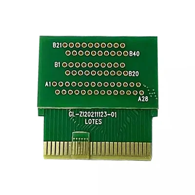
Metal detector pcb circuit board
Name: metal detector pcb circuit board
Type: Multilayer circuit board
Layers: 4 layers
Substrate: FR-4 TG150. 170.180
Copper thickness: 0.5-6.0mm
Plate thickness: 0.5-7.0mm
Hole size: 0.1mm
Surface treatment: ENIG, HASL, OSP, ENEPIG, flash gold
Board size: 52x67mm
Product name: circuit board PCBA assembly
Solder mask color: blue, green, red, black, white, etc.
Testing Services: AOI X-ray Functional Testing
Layers: 1-32 layers
Name: Multilayer Immersion Gold PCB
Type: Rigid PCB
Copper thickness: 1/3OZ~6 OZ
Application: Electronics
Packing: vacuum packing
Quality certification: ISO9001, ISO14001, TS16949, RoHs
- PCB Manufacturing Equipment

PCB Drilling machine

PCB pattern plating line

PCB solder mask expose machine

PCB pattern expose machine

Strip film etching line

Solder mask screen silk print machine

Solder mask scrubbing line
")
PCB Flying Probe Test (FPT)

Fully automatic exposure machine

High-standard confidentiality measures, signing confidentiality agreements, and all documents exporting must be approved to ensure that 100% of documents are not leaked.

we provide 24-hour service and support, you will receive a reply to your question within 2 hours and a quotation within 24 hours.

We can provide you with high frequency, high TG, high CTI, buried blind via, aluminum based PCB manufacturing, the quality is fully compliant with IPC 610-D standard, testing and quality assurance

With more than 20 years of industry experience, technology and production capacity are constantly increasing, and we can provide one-stop services from standard PCB to HDI PCB, high frequency and high...

Kingford has stable material suppliers with ten years of cooperation, such as Shengyi Technology, ITEQ, ROGERS, AGC, DUPONT, Doosan, Mitsubishi, etc.
Detailed processing of PCB Gold Finger:1) For PCB boards that need to be plugged in frequently, gold...
Golden finger function: ① If Shen Jin+Gold -plating finger process is made, the welding of double -s...
Golden fingers are connected parts between the memory slot and the memory slot, and all the signals ...
Golden fingers are connected parts between the memory slot and the memory slot, and all the signals ...
The principle of high -frequency oscillator detecting metalAdjusting the gain potentiometer of the h...
Golden finger classification1. Conventional gold finger (Qiping finger)Located on the edge of the pl...