

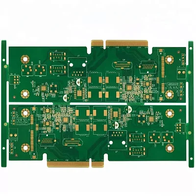
Gold Finger Printed PCB
Name: Gold Finger Printed PCB
Substrate: FR-4/High TG
Copper Thickness: 1 oz
Plate thickness: 1.6mm
minute. Hole size: 0.2mm
minute. Line width: 0.1mm/4mil
minute. Line spacing: 0.1mm/4mil
Surface treatment: ENIG
Impedance Control: 50/90/100±10% ohm
TG value: T170
Material flame retardant: 94v0
Standard: IPC-A-610G CLASS II&III
PCB Gold Finger Details processing
1. In order to increase the abrasion resistance of the golden fingers, gold fingers usually require electroplating hard gold (gold compounds).
2. Golden fingers need to fall backwards, usually 45 °, other angles such as 20 °, 30 °, etc. If there is no backward angle in the design, there is a problem; the 45 ° chamness in PCB
3. Golden fingers need to do a whole welded window. PIN does not need to open the steel net;
4. Shenxi and Shenyin pads need to be 14mil at the minimum distance from the top of the fingers; it is recommended to design more than 1mm from the finger position during design, including over -pore pads;
5. Do not spread copper on the surface of the golden finger;
6. All levels of the inner layer of the golden fingers need to be cut copper -cutting, usually 3mm in copper -cutting width; you can do half -finger copper cutting and the entire finger copper cutting.
Name: Gold Finger Printed PCB
Substrate: FR-4/High TG
Copper Thickness: 1 oz
Plate thickness: 1.6mm
minute. Hole size: 0.2mm
minute. Line width: 0.1mm/4mil
minute. Line spacing: 0.1mm/4mil
Surface treatment: ENIG
Impedance Control: 50/90/100±10% ohm
TG value: T170
Material flame retardant: 94v0
Standard: IPC-A-610G CLASS II&III
- Previous:Gold Finger Metal Detector PCB
- Next:8-layer Goldfinger PCB
