

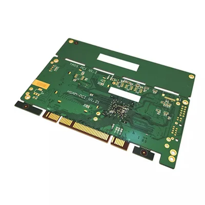
Goldfinger PCB
Name: Goldfinger PCB
Layers: 1-32 layers
Finished hole size: PTH ±0.003'', NPTH ±0.002"
Aspect Ratio: Minimum 1:8
Screen printing minimum line width: 0.006" or 0.15mm
Impedance control: ±5%
Ring: Min. 0.1mm
Solder Mask Registration: ±0.003"
Layer-to-layer registration: ±0.003"
Minimum copper-plated drill bit: 0.25mm, 0.30mm
Copper thickness: 1/2OZ 1OZ 2OZ 3OZ
Hole size: 0.2mm
Substrate: FR4 CEM1 CEM3 Aluminum
Plate thickness: 0.2mm-4.5mm
Surface treatment: HASL-LF/OSP/ENIG etc.
Golden finger classification
1. Conventional gold finger (Qiping finger)
Located on the edge of the plate neatly arranged the same length and width rectangular pad. It is often used in types of network cards and graphics cards. These gold fingers are more.
2. Long and short gold fingers (that is, the finger of the unconcerned gold)
Located rectangular pads with different lengths of the board, commonly used in the actual objects such as memory, U disk, card reader and other types.
3. Segmental golden fingers (intermittent gold finger)
The rectangular pad with different lengths of the plate side is cut off in the front.
Name: Goldfinger PCB
Layers: 1-32 layers
Finished hole size: PTH ±0.003'', NPTH ±0.002"
Aspect Ratio: Minimum 1:8
Screen printing minimum line width: 0.006" or 0.15mm
Impedance control: ±5%
Ring: Min. 0.1mm
Solder Mask Registration: ±0.003"
Layer-to-layer registration: ±0.003"
Minimum copper-plated drill bit: 0.25mm, 0.30mm
Copper thickness: 1/2OZ 1OZ 2OZ 3OZ
Hole size: 0.2mm
Substrate: FR4 CEM1 CEM3 Aluminum
Plate thickness: 0.2mm-4.5mm
Surface treatment: HASL-LF/OSP/ENIG etc.
