

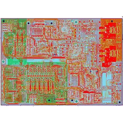
PCB design of integrated terminal
Name: PCB design of integrated terminal
Integrated terminal PCB design features:
1. Multi-module, dual-system system, powerful,
2. HiSilicon image coding comes with Android system,
3. Rockchip image decoding comes with Linux system.
PCB board parameters:
Number of PCB layers: 8 layers
PCB material: Htg170
PCB size: 185*124.5*1.6mm
Surface Treatment: Immersion Gold Process
PCB copper thickness: 1OZ
Minimum line width: 4MIL
Minimum line spacing: 4MIL
Minimum aperture: 8MIL
Impedance control: +/-10%
Photoelectric Multimedia PCB Design
Name: Photoelectric Multimedia PCB Design
Photoelectric multimedia circuit board design features:
Optoelectronic multimedia FPGA processor, 10G SFP optical port
Photoelectric multimedia PCB board parameters:
PCB name: 6 layers
PCB Category: Through Hole Board
PCB board: Htg170
Board size: 146.3*167.4*1.6mm
Surface Treatment: Immersion Gold Process
PCB copper thickness: 1OZ
Minimum line width: 5MIL
Minimum line spacing: 5MIL
Minimum hole diameter: 10MIL
Impedance control: +/-5%
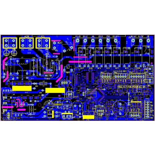
PCB design of digital set-top box
Name: PCB design of digital set-top box
Digital set-top box PCB design features:
1. Only some small filter capacitors are placed on the reverse side, and the device is placed on the other side;
2, DDR3, HDMI, etc. do not punch holes, the same layer processing;
3. The integrity of the ground plane and the handling of the ground loop are strictly guaranteed.
Digital set-top box PCB board parameters:
PCB name: 2 layers
PCB Category: Through Hole Board
PCB sheet: FR4 1oz
Veneer size: 171*128*1.6mm
Surface treatment: spray tin process
Minimum line width: 5MIL
Minimum line spacing: 5MIL
Minimum hole diameter: 12MIL
PCB design of industrial control motherboard
Name: PCB design of industrial control motherboard
Industrial control motherboard PCB design features:
1. High integration and high density, the holes on the BGA plate and the filter capacitors are changed to irregular shapes;
2. 25G high-speed signal, 10-degree angle wiring, adopting the 10-degree angle design recommended by Intel is a conventional method to solve the glass fiber effect.
PCB board parameters:
PCB name: 14 layers
PCB Category: Through Hole Board
PCB board: Htg70
PCB thickness: 2.0MM
Board size: 458*208MM
Surface treatment: Immersion gold process
PCB copper thickness: 1OZ
Minimum line width: 4MIL
Minimum line spacing: 4MIL
Minimum aperture: 8MIL
Impedance control: +/-5%
Multimedia motherboard PCB design
Name: Multimedia motherboard PCB design
Features: 1. The highest signal rate is 5G (optical port signal); 2. The grounding of the optical port casing has been specially treated to ensure that EMI affects the product.
Number of PCB layers: 10 layers
PCB board: Htg170, 1oz
PCB surface: immersion gold process
PCB parameters: 4/4mil, Via: 8mil
Impedance control: +/-5%
Power: 24VDC
Device interface: RS485*3 (dimming color sensor)
Network interface: RJ45*1 (100M)
Wireless communication: 4G *1 (full Netcom MQTT protocol) LORA *1
Output: DO *16 (220VAC@10A)
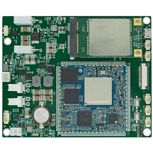
Six-layer core module PCB design
Name: Six-layer core module PCB design
Requirements: Length matching of data, address, clock, and packet-level processing
Number of PCB layers: 6 layers
PCB surface: immersion gold process
PCB board: Htg170, 1.6mm, 1oz
PCB parameters: 5/5mil, Via: 8mil
Impedance control: +/-10%
Power: 24VDC
Device interface: RS485*3 (dimming color sensor)
Network interface: RJ45*1 (100M)
Wireless communication: 4G *1 (full Netcom MQTT protocol) LORA *1
Output: DO *16 (220VAC@10A)
Amplifier: 60W audio amplifier
Storage: 512M DDR3 8G EMMC
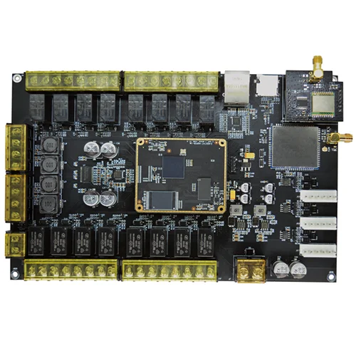
PCB Design of Intelligent Environment Controller
Name: PCB Design of Intelligent Environment Controller
Power: 24VDC
Device interface: RS485*3 (dimming color sensor)
Network interface: RJ45*1 (100M)
Wireless communication: 4G *1 (full Netcom MQTT protocol) LORA *1
Output: DO *16 (220VAC@10A)
Amplifier: 60W audio amplifier
Storage: 512M DDR3 8G EMMC
System: Linux
Relay output: remote control, timing control
Color matching function: 485 control color matching
Dimming function: 485 control dimming
RS485: Transparent transmission to collect sensor data
Network communication: The interface adopts MQTT consistently
Remote upgrade: support 4G, network port online upgrade
Lora communication: control downlink modules and sensors through lora
PCB Design of Chemical Air Detector
Name: PCB Design of Chemical Air Detector
Power supply: 7.4V3000mAh low temperature polymer lithium battery
Storage: RAM: 4G ROM: 64G
Device interface: TYPE-C (charging)
Wireless communication: whole network 2G\3G\4G + dual-band WIFI
Camera: 5 million autofocus camera
Screen: 5.7 inches 2160*1080 pixels
GPS: GPS+Beidou
On the communication protocol: TCP/IP
Printer: Embedded 58mm thermal printer
Card reading: embedded ID card information identification module
- PCB Design Capabilities
| PCB Design&Layout Capabilities | |||
| Min.trace width: | 2.5mil | Min.trace spacing | 2.5mil |
| Min.Vias: | 6mil(4mil laser drilling) | Max.layer | 48L |
| Min.BGA spacing | 0.35mm | Max.BGA Pin | 3600pin |
| Max.high-speed signal | 40 GBPS | Fastest delivery time | 6 Hours/ Item |
| HDI Highest layer | 22 L | HDI Highest layer | 14 L any layer HDI |
| PCB Design&Layout lead time | |||
| Number of pins on the board | 0-1000 | Design lead time (working days) | 3-5 days |
| 2000-3000 | 5-8 days | ||
| 4000-5000 | 8-12 days | ||
| 6000-7000 | 12-15 days | ||
| 8000-9000 | 15-18 days | ||
| 10000-12000 | 18-20 days | ||
| 13000-15000 | 20-22 days | ||
| 16000-18000 | 22-25 days | ||
| 18000-20000 | 25-30 days | ||
| Ultimate delivery capacity | 10000Pin/7 days | ||
| PS: The above delivery date is the regular delivery date, and the accurate design delivery date needs to be comprehensively evaluated according to the number of components, difficulty, layers and other factors of the circuit board! | |||

System advanced training, from beginners to experts, there are various technical special trainings every week.

Self-developed tool software and strict quality control system to ensure a successful one-time board opening

Parallel design to shorten lead time, conventional can shorten PCB design time by 50%

The maximum design scale is 90000pin, which can provide HDI/Any layer PCB design, 3D PCB design, RF design, 56G high-speed design, etc.

With a strict quality system process and a strict review system, we have zero error rate quality requirements for PCB design.

PCB design team with an average of more than 12 years of work experience, with complete design software, such as Cadence Allegro\ORCAD, Mentor WG\PADS, etc.

High-standard confidentiality measures, signing confidentiality agreements, and all documents exporting must be approved to ensure that 100% of documents are not leaked.

we provide 24-hour service and support, you will receive a reply to your question within 2 hours and a quotation within 24 hours.
PCB terminal blocks make it easy and safe to transfer signals, data and power to the PCB. They are s...
The optoelectronic printed circuit board is a new generation of packaging substrate with high comput...
A digital TV set-top box is a conversion device that converts digital TV signals into analog signals...
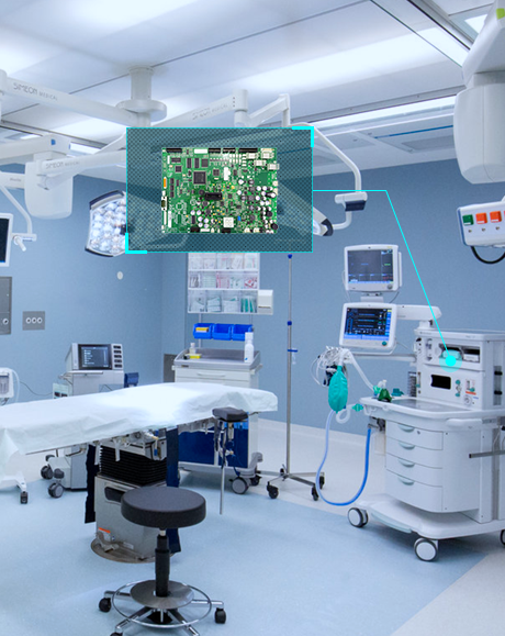
Industrial control product PCB. Circuit boards in electrical equipment that control the normal opera...
SIM: supportProcessor: Intel® Haswell-SChipset: H81Display: VGA HDMILAN: 1Memory: DDR3LStorage: M-SA...
CPUThe CPU is the most important part of the core board, consisting of an arithmetic unit and a cont...


Yes, we can provide free DFM service.
We know the importance of time, so we process standard PCB designs in a timely manner when we receive customer information.
Design specifications, design instructions, customer design requirements and related CHECKLIST, and provide layout files and structure files for customers to conduct layout review
With over 20 years of experience in handling different kinds of PCBs, our state-of-the-art equipment and team of experts provide significant advantages.
