

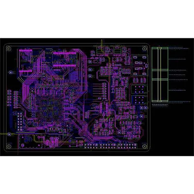
Communication Rigid RF PCB Design
Name: Communication Rigid RF PCB Design
Designable layers: 1-32 layers
Minimum line width and line spacing: 3mil
Minimum laser aperture: 4mil
Minimum mechanical aperture: 8mil
Copper foil thickness: 18-175цm (standard: 18цm35цm70цm)
Peel strength: 1.25N/mm
Minimum punching hole diameter: single side: 0.9mm/35mil
Minimum hole diameter: 0.25mm/10mil
Aperture tolerance: ≤φ0.8mm±0.05mm
Hole tolerance: ±0.05mm
Hole wall copper thickness: double-sided/multi-layer: ≥2um/0.8mil
Hole resistance: double-sided/multi-layer: ≤300цΩ
Minimum line width: 0.127mm/5mil
Minimum pitch: 0.127mm/5mil
Screen printing color: black, white, red, green, etc.
Surface treatment: lead/lead-free tin spray, ENIG, silver, OSP
Service: Provide OEM service
Certificate: ISO9001.ROSH.UL
RF printed circuit boards are also capable of supporting high bandwidth transmission of data systems. This makes them the darlings of the communications industry.
RF PCBs are also used to make remote controls that facilitate wireless communication.
Communication satellites are also manufactured using RF PCBs. Typically, they are used to convey information under thermally and environmentally unfriendly conditions.
With RF PCBs, it is guaranteed that such fluctuations will not affect performance.
Another common application area for RF PCBs in the industry is the manufacture of smartphones
Name: Communication Rigid RF PCB Design
Designable layers: 1-32 layers
Minimum line width and line spacing: 3mil
Minimum laser aperture: 4mil
Minimum mechanical aperture: 8mil
Copper foil thickness: 18-175цm (standard: 18цm35цm70цm)
Peel strength: 1.25N/mm
Minimum punching hole diameter: single side: 0.9mm/35mil
Minimum hole diameter: 0.25mm/10mil
Aperture tolerance: ≤φ0.8mm±0.05mm
Hole tolerance: ±0.05mm
Hole wall copper thickness: double-sided/multi-layer: ≥2um/0.8mil
Hole resistance: double-sided/multi-layer: ≤300цΩ
Minimum line width: 0.127mm/5mil
Minimum pitch: 0.127mm/5mil
Screen printing color: black, white, red, green, etc.
Surface treatment: lead/lead-free tin spray, ENIG, silver, OSP
Service: Provide OEM service
Certificate: ISO9001.ROSH.UL
