One - stop Electronic Manufacturing Services(EMS) Solution provider
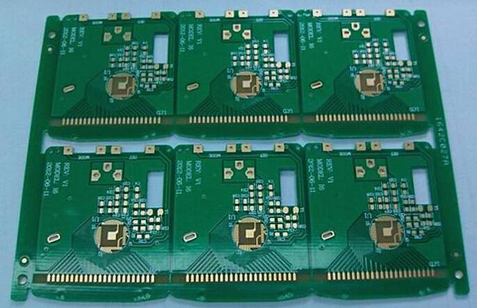
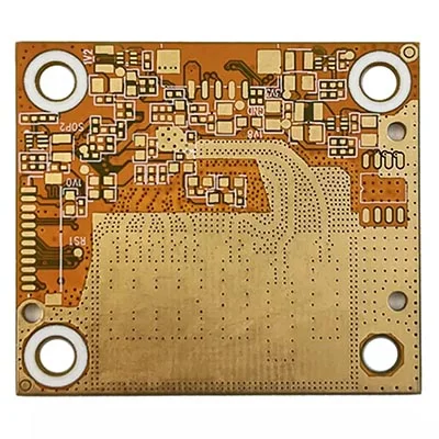
Electronic RF Printed Circuit Board
Name: Electronic RF Printed Circuit Board
Type: home appliance pcba
Brand name: JRK, pcba/fpcb
Copper Thickness: 1 oz
Surface treatment: HASL lead free
Minimum aperture: 0.25mm
Minimum line spacing: 0.003"
Material: FR-4
Layers: 2 layers
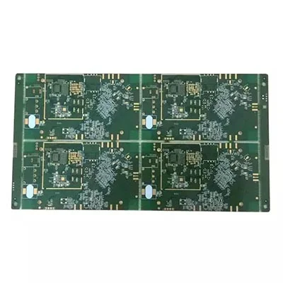
Name: Rogers 4003 RF Circuit Board
Model: High Frequency PCB-001
Type: Multilayer circuit board
Brand Name: ODM and OEM
Layers: 6 layers
Substrate: Rogers
Copper Thickness: 0.5oz-5oz
Plate thickness: 0.1 - 4mm
Surface treatment: HASL, ENIG, Immersion Silver, Immersion Tin, OSP
Board size: customized
Solder mask: yellow etc.
Silkscreen: white
Name: RF boost circuit board
Substrate: FR-4/Aluminum/Ceramic/cem-3
Copper Thickness: 0.5oz-8oz
Plate thickness: 0.2mm - 7mm
minute. Hole size: 0.02mm
minute. Line width: 0.003"
minute. Line Spacing: 0.003"
Surface treatment: HASL lead free
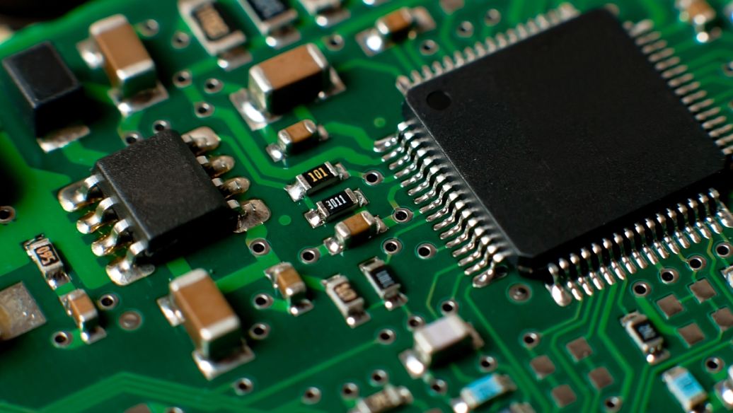
Product Name: Printed Circuit Board
Certificate: RoSH ISO/TS16949
Application: Electronic Equipment
Solder mask color: white black yellow green red
Material: FR4 CEM1 CEM3 High TG
Testing services: ICT, AOI, X-ray, functional testing
Silk screen color: black.white.yellow
Name: Rogers RO3003 RF PCB
Type: consumer electronics pcba
Copper Thickness: 1 oz, 1 oz
Applications: Electronics/Communications, Computers, Medical, Automotive
Service: PCB/PCBA/SMT/Component Sourcing
Solder mask color: blue, green, red, black, white, etc.
Testing Services: AOI X-ray Functional Testing
Certificate: ROHS/ISO9001
Substrate: FR-4/Hi-Tg/HDI/High Frequency Board/Copper Substrate
Plate thickness: 1.6mm
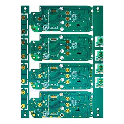
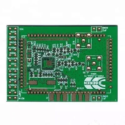
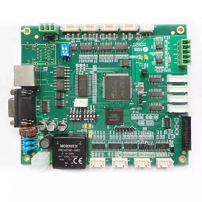
RF RC Helicopter Controller PCB
Name: RF RC Helicopter Controller PCB
Model: HX-007-729
Test Service: Flying Probe Test
Type: electronic board
Packing: anti-static bubble bag
Solder Mask Color: Green, White, Black
Layers: 1-58 layers
Certificate: ISO9001/RoHS/CE
Service: OEM
Usage: home appliance accessories
Name: RF Half Hole PCB
Substrate: FR4, High TG FR4, High Frequency, Alum, FPC
Copper Thickness: 0.5-4 0z
Plate thickness: 0.1-4mm±10%
minute. Hole Size: 0.0078" (0.2mm)
minute. Line width: 0.003 in (0.075 mm)
minute. Line Spacing: 0.003" (0.075mm)
Surface treatment: HASL, ENIG, Immersion Silver, Immersion Tin, OSP
Board size: square, round, irregular (with fixture)
Services: PCB and PCB Assembly
Layers: 1-48
PTH hole tolerance: ±0.002 in (0.005 mm)
Minimum Soldermask Gap: 0.003" (0.07mm)
Screen printing minimum size: 0.006"0.15mm)
Maximum size of decorative panel: 700*460mm
PCB shape: square, round, irregular (with fixture)
Subcomponents: plastic, metal, screen
Certificate: IATF16949, ISO13485, ISO9001, ISO14001
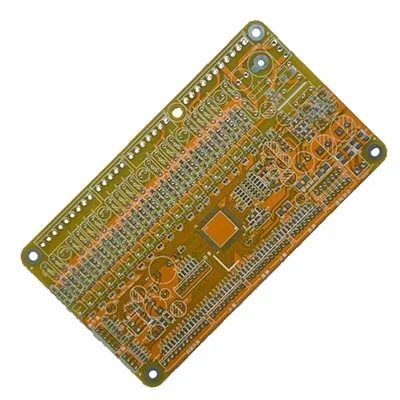
Name: HDI PCB RF Circuit Board
Layers: 2 layers
Substrate: FR-4
Copper Thickness: 1 oz
Plate Thickness: 1.6mm, 1.6mm
Hole size: 0.1mm
Line width: 3 mm
Line spacing: 3 mm
Surface treatment: spray tin lead-free, spray tin lead-free
Minimum aperture: 0.25mm
Minimum line spacing: 0.003"
Color: Green or as your request
Name: Rogers 4003 RF PCB
Substrate: Rogers 4003
Copper Thickness: 1.0mm
Plate Thickness: 1.6mm
minute. Hole size: 0.1mm
minute. Line width: 0.1mm
minute. Line spacing: 0.1 mm
Item: High Frequency PCB Rogers 4003 RF PCB for RF
Maximum processing area: 680×1000MM
Layers: 1-28 layers
Silk screen color: black, white, red, green
Finished board: thickness≤1.0MM, tolerance: ±0.1MM
Twist and Bend: ≤ 0.75%, Min: 0.5%
TG range: 130 - 215℃
Certificate: ISO9001.ROSH.UL
- PCB manufacturing equipment
- PCB manufacturing capability

PCB Drilling machine

PCB pattern plating line

PCB solder mask expose machine

PCB pattern expose machine

Strip film etching line

Solder mask screen silk print machine

Solder mask scrubbing line
")
PCB Flying Probe Test (FPT)

Fully automatic exposure machine
| Standard PCB Production Capability | |
| Feature | Capability |
| Quality Grade | Standard IPC 2 |
| Number of Layers | 1 - 32layers |
| Order Quantity | 1pcs - 10,000,000 pcs |
| Build Time | 2days - 5weeks (Expedited Service) |
| Material | FR-4 Standard Tg 150°C, FR4-High Tg 170°C, FR4-High-Tg 180°C, FR4-Halogen-free, FR4-Halogen-free & High-Tg |
| Board Size | Min 6*6mm | Max 600*700mm |
| Board size tolerance | ±0.1mm - ±0.3mm |
| Board Thickness | 0.4mm - 3.2mm |
| Board Thickness Tolerance | ±0.1mm - ±10% |
| Copper Weight | 0.5oz - 6.0oz |
| Inner Layer Copper Weight | 0.5oz - 2.0oz |
| Copper Thickness Tolerance | +0μm +20μm |
| Min Tracing/Spacing | 3mil/3mil |
| Solder Mask Sides | As per the file |
| Solder Mask Color | Green, White, Blue, Black, Red, Yellow |
| Silkscreen Sides | As per the file |
| Silkscreen Color | White, Blue, Black, Red, Yellow |
| Surface Finish | HASL - Hot Air Solder Leveling |
| Lead Free HASL - RoHS | |
| ENIG - Electroless Nickle/Immersion Gold - RoHS | |
| ENEPIG - Electroless Nickel Electroless Palladium Immersion Gold - RoHS | |
| Immersion Silver - RoHS | |
| Immersion Tin - RoHS | |
| OSP -Organic Solderability Preservatives - RoHS | |
| Min Annular Ring | 3mil |
| Min Drilling Hole Diameter | 6mil, 4mil-laser drill |
| Min Width of Cutout (NPTH) | 0.8mm |
| NPTH Hole Size Tolerance | ±.002" (±0.05mm) |
| Min Width of Slot Hole (PTH) | 0.6mm |
| PTH Hole Size Tolerance | ±.003" (±0.08mm) - ±4mil |
| Surface/Hole Plating Thickness | 20μm - 30μm |
| SM Tolerance (LPI) | .003" (0.075mm) |
| Aspect Ratio | 1.10 (hole size: board thickness) |
| Test | 10V - 250V, flying probe or testing fixture |
| Impedance tolerance | ±5% - ±10% |
| SMD Pitch | 0.2mm(8mil) |
| BGA Pitch | 0.2mm(8mil) |
| Chamfer of Gold Fingers | 20, 30, 45, 60 |
| Other Techniques | Gold fingers |
| Blind and Buried Holes | |
| peelable solder mask | |
| Edge plating | |
| Carbon Mask | |
| Kapton tape | |
| Countersink/counterbore hole | |
| Half-cut/Castellated hole | |
| Press fit hole | |
| Via tented/covered with resin | |
| Via plugged/filled with resin | |
| Via in pad | |
| Electrical Test | |

We have the most competitive price, our own factory, reasonable cost control, no hidden cost

We have state-of-the-art equipment required for manufacturing and assembly

we provide 24-hour service and support, you will receive a reply to your question within 2 hours and a quotation within 24 hours.

Before the official production of the PCB, we will conduct a free DFM review service and support free Allegro, Altium, Protel, PADS, OBD, Gerber and other formats.
什么是电子产品中的射频?射频 (RF) 是表示电磁辐射频谱或电磁无线电波的振荡速率的测量值,频率范围从 300 吉赫 (GHz) 到低至 9 千赫 (kHz)。
Ideal choice of multi -layer board (MLB) structureThe manufacturing cost of FR-4 and other processes...
RF is called RF, RF is RF current, which is the abbreviation of an electromagnetic wave of high -fre...
The ceramic filling PTFE composite material used for Rogers RO3003 is resistant to high temperature,...
The application of radio frequency technology in industrial field data can reduce transmission costs...
Half -hole plating is a cost -effective connection strategy that converts the circuit board into sub...