One - stop Electronic Manufacturing Services(EMS) Solution provider

Basic knowledge of pcb design entry
Basic knowledge of pcb design entry
In high-speed design, the continuity of controlled impedance board and line impedance is a very important issue. The common impedance is 50 ohms for single-ended and 100 ohms for differential. How to ensure signal integrity? In our usual way, the adjacent layers of the signal line have a complete GND plane, or a power plane. We use single-chip microcomputers to make products. Under normal circumstances, we don't need to make impedance, and its working frequency is generally very low. You can Baidu SI9000 to learn the method of impedance calculation. Xiaobei generally doesn't pay much attention to this issue, and the impedance is calculated by the board factory for us. Let's learn the basics of PCB design with Xiaobei.
setting skills
Different settings need to be made at different stages of the design. In the layout stage, large grid points can be used for device layout; for large devices such as ICs and non-positioning connectors, 50~100mil grid point accuracy can be selected for layout, while for resistors, capacitors and Small passive devices such as inductors can be laid out with a grid of 25mil. The precision of the large lattice point is conducive to the alignment of the device and the aesthetics of the layout. In high-speed wiring, we generally use mm as the unit, and most of us use mil as the unit.
PCB layout rules
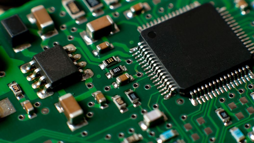
1. Under normal circumstances, all components should be arranged on the same surface of the circuit board as much as possible. Only when the top layer components are too dense can some devices with limited height and low heat generation, such as chip resistors, chip capacitors, and Chips, etc. are placed on the bottom layer.
2. Under the premise of ensuring electrical performance, the components should be placed on the grid and arranged parallel or vertically to each other in order to be neat and beautiful; the arrangement of the components should be compact, and the components should be evenly distributed and densely distributed on the entire layout.
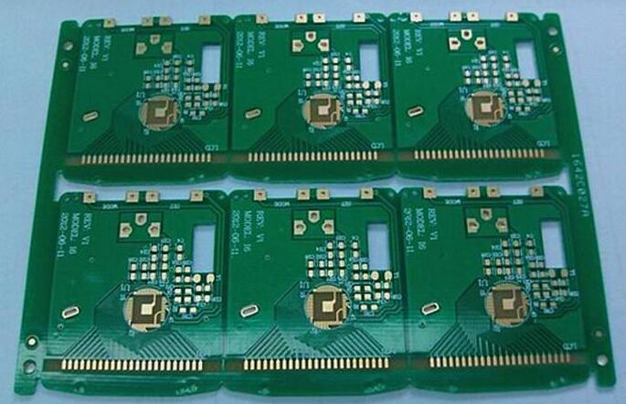
3. The distance between the device and the edge of the circuit board is generally not less than 2mm, and the process is that the distance between the device and the device is 5mm. When it is less than 5mm, we should process the process edge. Of course, the mechanical strength that the circuit board can withstand must also be considered.
Layout Tips
In the layout design of the PCB, the units of the circuit board should be analyzed, and the layout design should be carried out according to the function. When laying out all the components of the circuit, the following principles should be complied with:
1. Arrange the position of each functional circuit unit according to the circuit flow, make the layout convenient for signal circulation, and keep the signal in the same direction as possible.
2. Take the core components of each functional unit as the center and make layout around it. Components should be evenly, integrally and compactly arranged on the PCB, minimizing and shortening the leads and connections between components. When the interface is fixed, we should start from the interface, and then lay out the core components. The shortest high-speed signal is the principle.
3. For circuits operating at high frequencies, the distribution parameters between components must be considered. The low-frequency and high-frequency circuit circuits should be separated, and the digital and analog circuits should be designed separately.
layout design
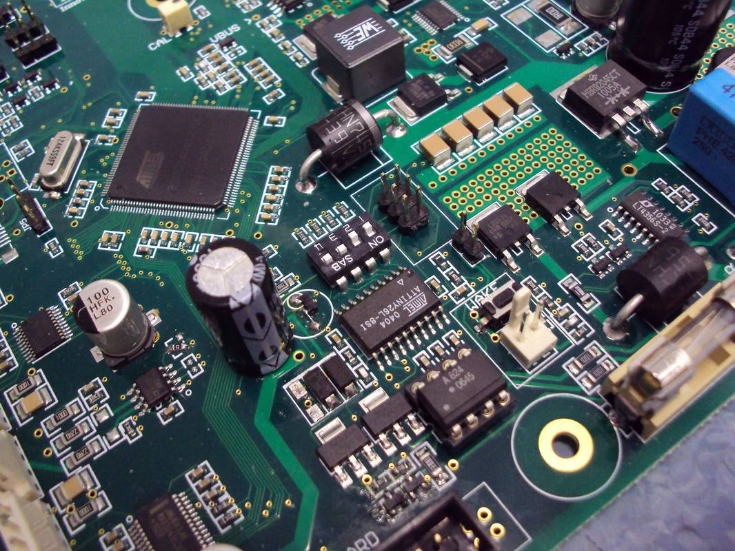
In PCB, special components refer to key components in the high frequency part, core components in the circuit, components susceptible to interference, components with high voltage, components with high heat generation, and some heterosexual components , The position of these special components needs to be carefully analyzed, and the layout should meet the requirements of circuit function and production requirements. Improper placement of them may cause circuit compatibility issues, signal integrity issues, and lead to PCB design failure.
Placement order
1. Place components that are closely matched with the structure, such as power sockets, indicator lights, switches, connectors, etc.
2. Place special components, such as large components, heavy components, heating components, transformers, ICs, etc.
3. Place small components.
layout check
1. Whether the size of the circuit board is consistent with the processing size required by the CAD drawing.
2. Whether the layout of the components is balanced, neatly arranged, and whether they have all been laid out.
3. Whether there is any conflict at all levels. Such as components, frames, connectors are reasonable.
4. Whether the commonly used components are easy to maintain and install. Such as switches, plug-in board insertion equipment, components that must be replaced frequently, etc.
5. Is the distance between heat sensitive components and heating components reasonable?
6. Whether the heat dissipation is good.
7. Whether the line interference problem needs to be considered.
Wiring principles
1. Avoid arranging important signal lines on the edge of the PCB, such as clock and reset signals.
2. The distance between the chassis ground wire and the signal wire is at least 2mm
3. The high-speed signal should be drilled as small as possible to ensure the integrity of the signal.
4. Whether the digital and analog signals are separated. Whether high frequency and low frequency signals are separated.
5. When designing large-area copper cladding, there should be windows on the copper cladding, add cooling holes, and design the windows into a mesh shape.
6. Oscillating crystal, whether there is wiring under the transformer. These introductory basics can only be improved every day if we practice hard.
silk screen display
1. The silk screen bit number is not on the solder mask, and it is missing after placing the silk screen production.
2. The silk screen position number is clear, and the recommended character width/height size is 4/25mil, 5/30mil, 6/45mil.
3. Maintain the uniformity of direction. Generally, there should not be more than two directions on a PCB. It is recommended that the letters be on the left or at the bottom
Network DRC check and structure check
Quality control is an important part of the PCB design process. General quality control methods include: design self-inspection, design mutual inspection, expert review meeting, special inspection, etc.
The schematic diagram and structural element diagram are the most basic design requirements. The network DRC inspection and structural inspection are to confirm that the PCB design meets the two input conditions of the schematic netlist and structural element diagram respectively.
regular assembly
In the design, from the perspective of PCB board assembly, the following parameters should be considered:
1. The diameter of the hole should be determined according to the maximum material condition (MMC) and the minimum material condition (LMC). The diameter of the hole of an unsupported component should be selected such that the MMC of the pin is subtracted from the MMC of the hole, and the resulting difference is between 0.15 -0. 5mm. And for ribbon leads, the difference between the nominal diagonal of the lead and the inner diameter of the unsupported hole shall not exceed 0.5mm and shall not be less than 0.15mm.
2. Place smaller components reasonably so that they will not be covered by larger components.
3. The thickness of the solder mask should not be greater than 0.05mm.
4. The screen printed logo cannot intersect with any pad.
5. The upper half of the circuit board should be the same as the lower half to achieve structural symmetry. Because asymmetrical boards may become warped.
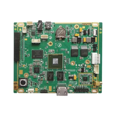
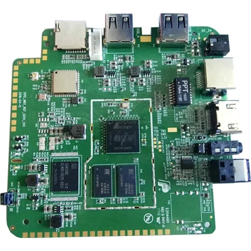
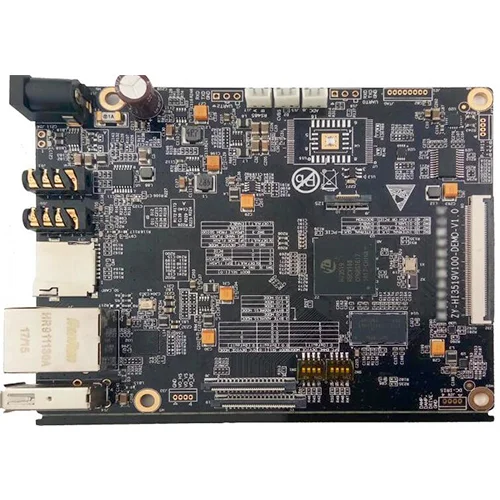
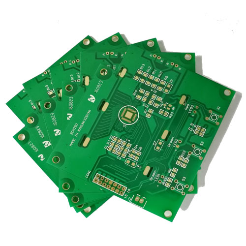
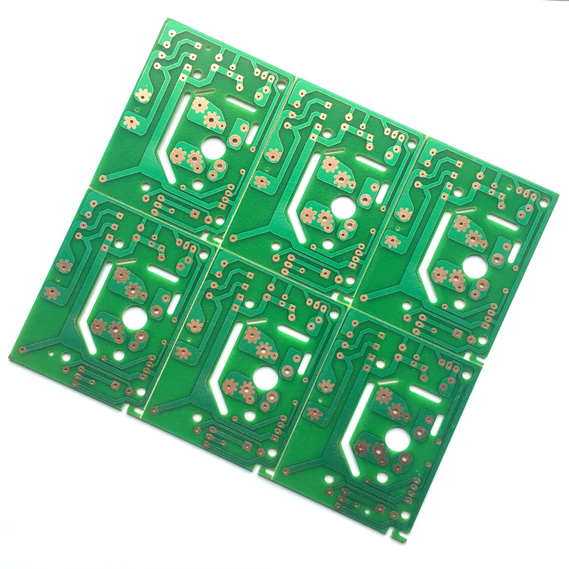
You can download a PCB from the Internet for comparison based on the basic knowledge above. We can also look to optimize an off-the-shelf board.
- Previous:PCB Assembly Guidelines
- Next:No