One - stop Electronic Manufacturing Services(EMS) Solution provider

The specific steps and composition of printed circuit board (PCB)
The specific steps and composition of printed circuit board (PCB)
With the improvement of microelectronics technology and industrial manufacturing level, printed circuit board (PCB) has become the basic unit of all smart devices and systems. PCB can realize the wiring and electrical connection or electrical connection between various electronic components such as integrated circuits. Insulation, providing the required electrical characteristics, providing solder mask graphics for automatic welding, and providing identification characters and graphics for component insertion, inspection, and maintenance.
1. The general steps of PCB
The design of the printed circuit board is based on the circuit schematic diagram to realize the functions required by the circuit user. The design of the printed circuit board mainly refers to the layout design, which requires the layout of internal electronic components, metal wiring, through holes and external connections. , point protection, heat dissipation, crosstalk and other factors, excellent circuit design can save production cost, achieve good circuit performance and heat dissipation performance, simple layout design can be realized by hand, but complex circuit design is generally not It needs to be realized with the help of computer aided design (CAD).
Famous design software includes OrCAD, Pads (ie PowerPCB), Altium Designer, FreePCB, CAM3501, etc. When designing circuit boards, first of all, the pin size and structure package form of all components in electronic production should be marked with detailed and real specific numbers. It should be noted that sometimes the perineal manufacturers of the same type of components have different values and pin arrangements;
Secondly, according to the designed electrical schematic diagram, simulate the overall block diagram of the components; finally, according to the block diagram and electrical requirements, in the sketch of the circuit board, when drawing the detailed pins of each component and their positions on the circuit board, care should be taken The size of components and the distance between them, the size of peripheral components from the edge, input and output, grounding and power lines, high-frequency circuits, signal lines that are prone to radiation and interference, etc.
2. Composition of PCB
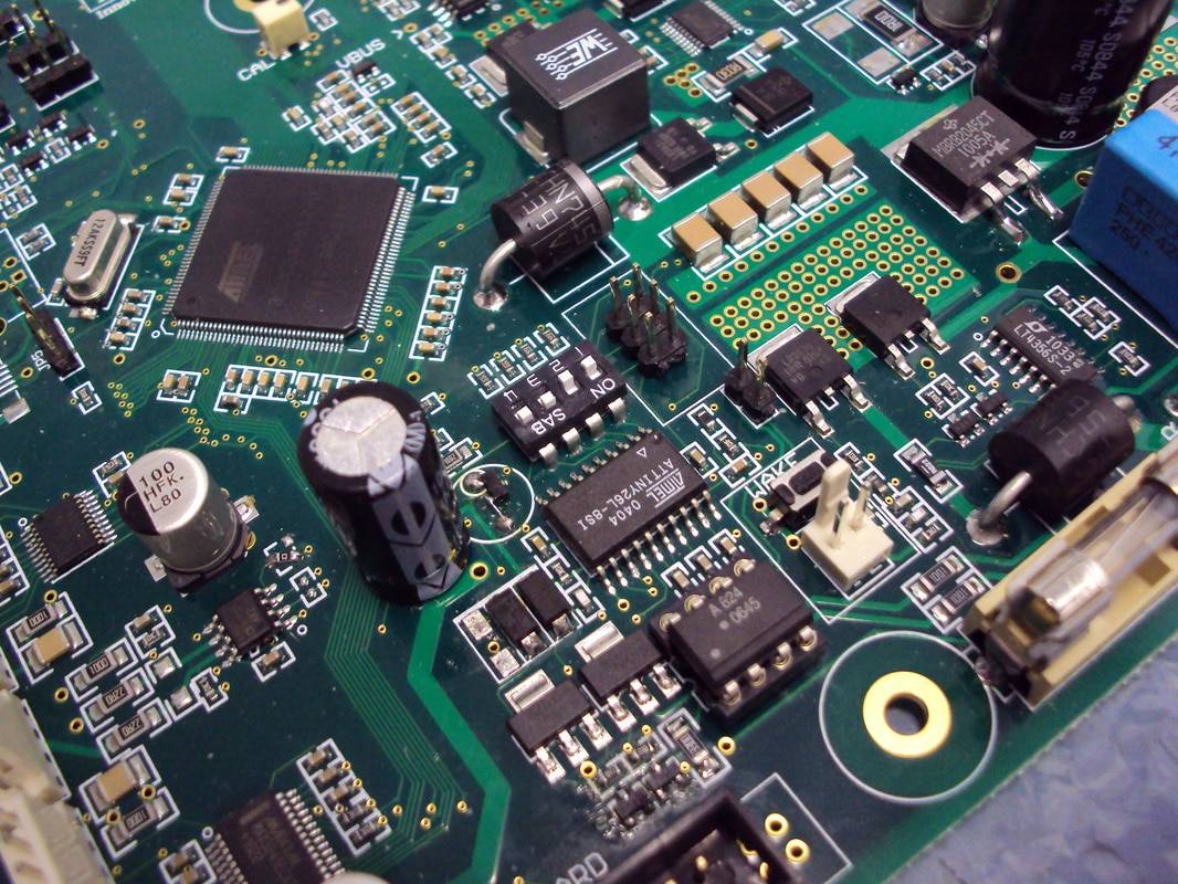
1) Line and drawing (Pttern): The line is used as a tool for the conduction between the original components. In the design, a large copper surface is additionally designed as the grounding and power layer. The line and the drawing are made at the same time.
2) Dielectric layer (Dielectric): It is used to maintain the insulation between lines and layers, commonly known as the substrate.
3) Trough hole/via: The via hole can make the lines of more than two levels conduct each other, the larger via hole is used as a component plug-in, and the non-conducting hole (nPTH) is usually used as a Surface mount positioning, used for fixing screws during assembly.
4) Solder resist ink (Soldcr resistant/Solder Mask): Not all copper surfaces have to eat tin parts, so the non-tin-eaten area will be printed with a layer of material (usually epoxy resin) that isolates the copper surface from eating tin , Avoid short circuit between non-tin-eaten lines. According to different processes, it is divided into green oil, red oil and blue oil.
5) Silk screen (Legend /Marking/Silk screen): This is a non-essential component. Its main function is to mark the name and position box of each part on the circuit board, which is convenient for maintenance and identification after assembly.
6) Surface Finish: Since the copper surface is easily oxidized in the general environment, it cannot be tinned (poor solderability), so it will be protected on the copper surface that eats tin. The protection methods include HASL, ENIG, Imersion Silver, Imersion Tin, and OSP. Each method has its advantages and disadvantages, and they are collectively referred to as surface treatment.
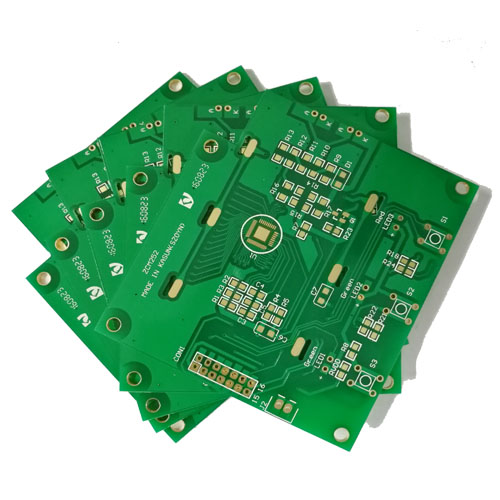
1. Printed circuit board (PCB)
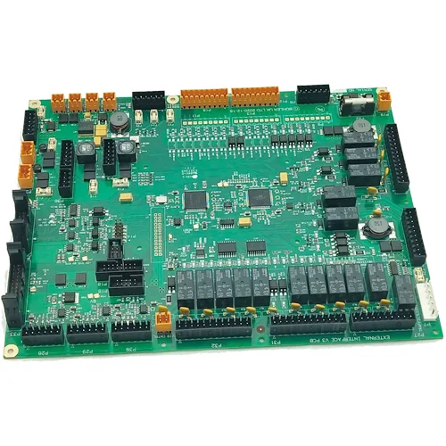
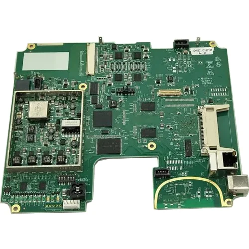
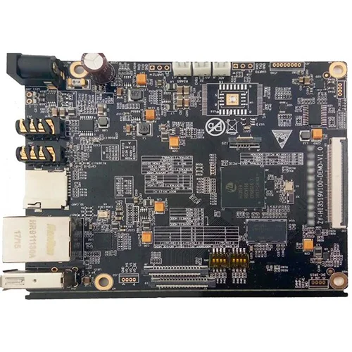
PCB is the abbreviation of Printed Circuit Board (Printed Circuit Board). Also known as printed circuit board, printed circuit board, because it is made by electronic printing, it is called "printed" circuit board. A printed circuit board is a substrate for assembling electronic components, and is a printed board that forms point-to-point connections and printed components on a general-purpose substrate according to a predetermined design. The main function of this product is to make various electronic components form a predetermined circuit connection and play the role of relay transmission. It is the key electronic interconnection of electronic products and is known as the "mother of electronic products". As the substrate and key interconnection of electronic parts, PCB is required for any electronic equipment or products.
2. The manufacturing principle of PCB
When we open the keyboard of a general-purpose computer, we can see a soft film (flexible insulating substrate), printed with silver-white (silver paste) conductive patterns and key patterns. Because this kind of pattern is obtained by the general screen printing method, we call this printed circuit board a flexible silver paste printed circuit board. However, the various computer motherboards, graphics cards, network cards, modems, sound cards and printed circuit boards on household appliances that we saw in the computer city are different. The base material it uses is made of paper base (often used for one side) or glass cloth base (often used for double-sided and multi-layer), pre-impregnated with phenolic or epoxy resin, one or both sides of the surface layer are glued with copper clad film and then laminated and cured made. This kind of circuit board copper clad sheet, we call it a rigid board. Then make a printed circuit board, we call it a rigid printed circuit board. We call single-sided printed circuit boards with printed circuit patterns on one side, and printed circuit boards with printed circuit patterns on both sides, and then the printed circuit boards formed by double-sided interconnection through metallization of holes are called double-sided boards. If a printed circuit board with one double-sided inner layer and two single-sided outer layers or two double-sided inner layers and two single-sided outer layers is used alternately through the positioning system and insulating bonding materials and The printed circuit boards in which the conductive patterns are interconnected according to the design requirements become four-layer and six-layer printed circuit boards, also known as multilayer printed circuit boards. Now there are more than 100 layers of practical printed circuit boards.
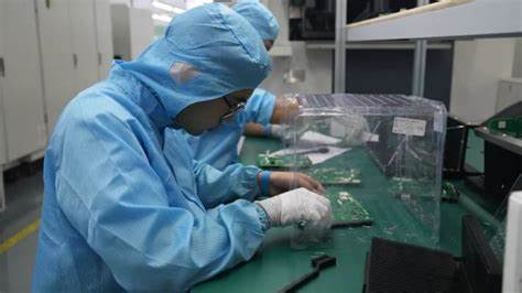
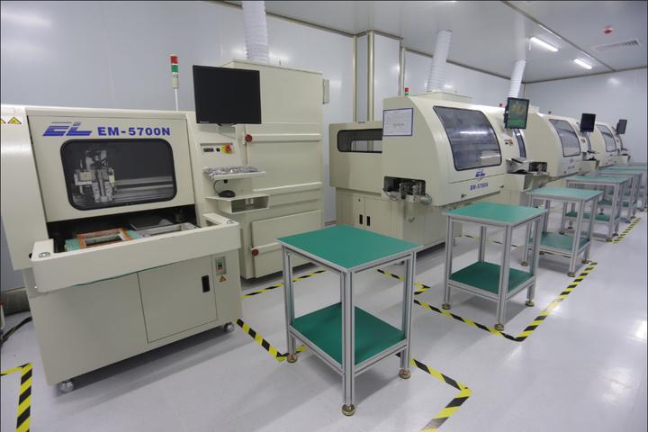
3. PCB production process
The production process of PCB is relatively complicated, and it involves a wide range of processes, from simple mechanical processing to complex mechanical processing, common chemical reactions, photochemical, electrochemical, thermochemical and other processes, computer-aided design CAM and other knowledge . Moreover, there are many technological problems in the production process and new problems will be encountered from time to time, and some problems will disappear without finding out the cause. Since the production process is a discontinuous assembly line, any problem in any link will cause the entire line to stop production Or the consequences of a large number of scrapping. If the printed circuit board is scrapped, it cannot be recycled and reused. The work pressure of process engineers is relatively high, so many engineers leave this industry and go to printed circuit board equipment or material suppliers to do sales and technical services. .
The substrate of the board itself is made of insulating and heat-insulating material that is not easy to bend. The small circuit material that can be seen on the surface is copper foil. Originally, the copper foil covered the entire board, but in the manufacturing process part It is etched away, and the remaining part becomes a network of fine lines. These lines are called conductors.
pattern) or wiring, and is used to provide circuit connections for parts on the PCB.
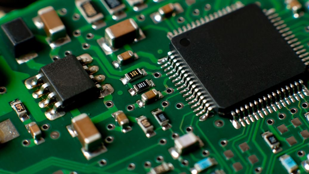
In order to fix the parts on the PCB, we solder their pins directly to the wiring. On the most basic PCB (single panel), the parts are concentrated on one side, and the wires are concentrated on the other side. In this way we It is necessary to make holes on the board so that the pins can pass through the board to the other side, so the pins of the parts are soldered on the other side. Because of this, the front and back sides of the PCB are called the component side (Component
Side) and welding surface (Solder Side).
If there are some parts on the PCB that need to be removed or put back after the production is completed, then the socket (Socket) will be used when installing the part. Since the socket is directly welded on the board, the parts can be disassembled and assembled arbitrarily .
If two PCBs are to be connected to each other, we generally use edge joints commonly known as "golden fingers".
connector). The gold finger contains many exposed copper pads, which are actually part of the PCB wiring. Usually, when connecting, we insert the gold finger on one of the PCBs into the appropriate slot on the other PCB (Generally called the expansion slot Slot). In the computer, such as a display card, sound card or other similar interface cards, are connected to the motherboard by golden fingers.
The green or brown on the PCB is the solder resist paint (solder
The color of the mask). This layer is an insulating protective layer that can protect the copper wire and prevent parts from being soldered to incorrect places. A layer of silk screen printing (silk) will be printed on the solder mask
screen). Usually, text and symbols (mostly white) are printed on it to mark the position of each part on the board. The screen printing surface is also called the icon surface (legend).
The printed circuit board etches the complex circuit copper wires between parts and parts on a board after careful and neat planning, providing the main support for electronic components during installation and interconnection, and is indispensable for all electronic products basic parts.
A printed circuit board is a flat plate made of non-conductive material, on which there are usually pre-drilled holes designed to install chips and other electronic components. The holes of the components help to electronically connect the pre-defined metal paths printed on the board. After the pins of the electronic components pass through the PCB, they are then adhered to the PCB with conductive metal welding rods to form a circuit.
4. Brief history and development direction of PCB
A brief history of development: my country began the development of single-sided printed boards in the mid-1950s, which were first used in semiconductor radios. In the mid-1960s, my country's foil-clad substrate was self-reliantly developed, making the copper foil etching method the leading process for PCB production in my country. In the 1960s, it was able to produce single-sided boards in large quantities. Production of double-sided metallized hole printing in small batches, and development of multi-layer boards in a few units. In the 1970s, the graphic electroplating and etching process was promoted in China, but due to various interferences, the special materials and special equipment for printed circuits did not keep up with it in time, and the entire production technology level lagged behind the foreign advanced level. In the 1980s, due to the introduction of the reform and opening up policy, not only a large number of single-sided, double-sided, and multi-layer printed circuit board production lines with foreign advanced levels in the 1980s were introduced, but also after more than ten years of digestion and absorption, it has improved rapidly. my country's printed circuit production technology level.

Development Direction: In recent years, China's electronics industry has become one of the main pillars driving domestic economic growth. With the rapid development of computers, communication equipment, consumer electronics and automobile industries,
The PCB industry has also achieved rapid development. With the development of printed circuit products, new materials, new technology and new equipment are required. While expanding output, my country's printed electrical material industry must focus on improving performance and quality; the printed circuit special equipment industry is no longer a low-level imitation, but is developing toward production automation, precision, multi-function, and modern equipment . PCB production integrates the world's high and new technologies. The printed circuit production technology will adopt new technologies such as liquid photosensitive imaging, direct electroplating, pulse electroplating, and laminated multi-layer boards.
Five, the characteristics and classification of PCB and upstream and downstream
PCB features six aspects: high density, high reliability, designability, manufacturability, assembleability and maintainability.
Generally speaking, the more complex the functions of electronic products, the longer the loop distance, and the more contact pins, the more layers the PCB requires, such as high-end consumer electronics, information and communication products, etc.; In curved products: such as notebook computers, cameras, automotive instruments, etc. According to the number of layers, PCB classification can be divided into single-sided board (SSB), double-sided board (DSB) and multi-layer board (MLB); according to softness, it can be divided into rigid printed circuit board (RPC) and flexible printed circuit board (FPC). In industrial research, generally according to the above basic classification of PCB products, the PCB industry is subdivided into six main subdivisions: single-sided board, double-sided board, conventional multilayer board, flexible board, HDI (high-density sintered) board, and packaging substrate. industry.
The PCB upstream industry includes suppliers of PCB substrate raw materials and PCB production equipment suppliers, and the downstream industry includes consumer electronics, computers and peripheral products, automobile industry and mobile phone industry. According to the industrial chain, it can be divided into raw materials - copper clad laminates - printed circuit boards - electronic product applications. The specific analysis is as follows:
Glass fiber cloth: Glass fiber cloth is one of the raw materials of copper clad laminates. It is woven from glass fiber yarn and accounts for about 40% (thick plate) and 25% (thin plate) of the cost of copper clad laminates. The glass fiber yarn is calcined into a liquid state by calcining silica sand and other raw materials in a kiln, and drawn into a very fine glass fiber through a very small alloy nozzle, and then hundreds of glass fibers are twisted into a glass fiber yarn.
Copper foil: Copper foil is the raw material that accounts for the largest proportion of the cost of copper clad laminates, accounting for about 30% (thick plate) and 50% (thin plate) of the cost of copper clad laminates. Therefore, the price increase of copper foil is the main driving force for the price increase of copper clad laminates.
Copper-clad laminate: Copper-clad laminate is a product of bonding glass fiber cloth and copper foil together with epoxy resin as a fusion agent. It is the direct raw material of PCB. It is made into a printed circuit after etching, electroplating, and lamination of multi-layer boards. plate.
- Previous: PCB circuit board (printed circuit board)
- Next:No