
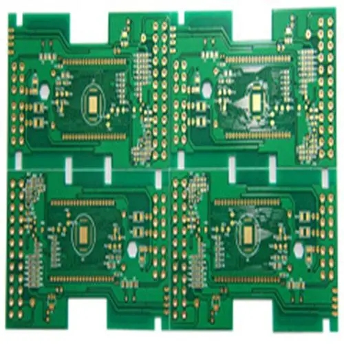
Professional PCB manufacturing and assembly
Building 6, Zone 3, Yuekang Road,Bao'an District, Shenzhen, China
+86-13410863085Mon.-Sat.08:00-20:00

SMT process and capacity, and the use of stencil thickness and principle
SMT process: short for Surface Mount Technology, SMT surface mount technology is an electronic assembly technology that originated in the 1960s, was initially developed by IBM in the United States, and then gradually matured in the late 1980s. SMT technology is to install electronic components, such as resistors, capacitors, transistors, integrated circuits, etc. on printed circuit boards, and form electrical connections through lead soldering. The components used are also referred to as SMD (surface mount devices). The biggest difference between SMT and plug-in technology is that SMT surface adhesion technology does not need to reserve corresponding through holes for the pins of components, and the component size of surface adhesion technology is much smaller than that of plug-in packaging. This SMT technology can greatly reduce the volume of electronic products to achieve the purpose of thin and short, referred to as SMT process.
Steel mesh thickness, principle and application in SMT process
The so-called Stencil is a very thin steel sheet. The size of the steel mesh is usually fixed to match the solder paste printing machine, but the thickness of the steel mesh varies from 0.08mm, 0.10mm, 0.12mm, 0.15mm, 0.18mm, etc.
The purpose of the stencil is to enable solder paste to be printed on the circuit board in the SMT chip processing process. Therefore, there will be many holes carved on the stencil. When printing solder paste, solder paste should be coated on the top of the stencil, while the circuit board will be placed below the stencil, and then a scraper (usually a scraper, because solder paste is like a toothpaste like viscous substance) will be used to brush the stencil with solder paste, When the solder paste is squeezed, it will flow down from the opening of the steel mesh and stick to the circuit board. After removing the steel mesh, it will be found that the solder paste has been printed on the circuit board. To put it simply, the steel mesh is like a cover to be prepared when painting, and the solder paste is equivalent to paint. The cover is engraved with the desired figure, and the desired figure will appear when you spray paint on the cover.
Since the stencil is used to print solder paste on the circuit board, the first step is to put the circuit board on the SMT production line, and then the stencil is used to print solder paste. The purpose of solder paste is usually to weld the parts on the circuit board, so as long as the position of the parts to be welded on the circuit board changes, a new steel mesh must be reopened.
The circuit board manufacturer and the circuit board designer will explain the SMT process and capability, the thickness of the steel mesh and the use of the principle
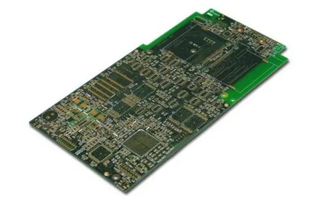
Circuit board assembly
Nov 04,2022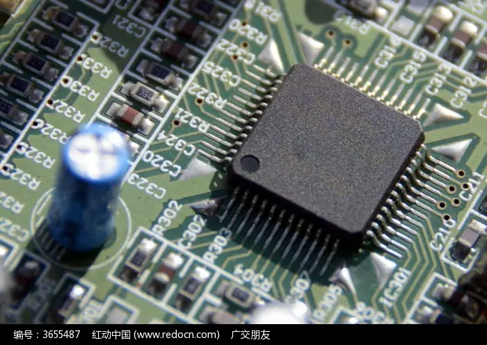


Just upload Gerber files, BOM files and design files, and the KINGFORD team will provide a complete quotation within 24h.