

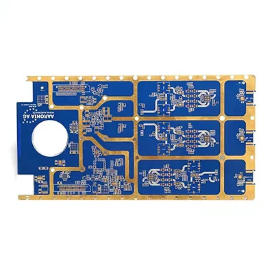
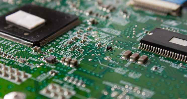
PCB Layout Guide: Effective component placement will result in wire routing
It is critical for board designers to lay out their boards to create the best possible signal and po...

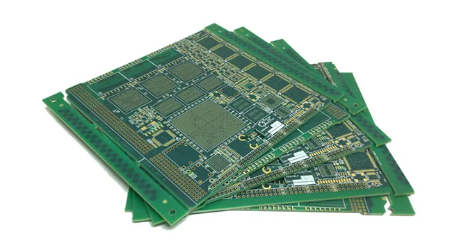
Kingford focus on the high-quality PCBA order demand of "Multiple varieties, medium and small batch, and short lead time".

It is critical for board designers to lay out their boards to create the best possible signal and po...
In addition to the machining technology, back drilling design and stump control also have some effec...

manufacturing technology and system complexity and other key factors have many conflicting requireme...

Poor insulation of copper wire will lead to arc between copper wire and copper wire. Too close betwe...

it is necessary to pay attention to the maintenance order so as to find the shortest path to solve p...
If there are a lot of key signals on the PCB to do impedance, you can attach a separate document, wi...
The other is ground (or low potential) noise, that is, ground noise caused by the potential differen...

high speed circuit design technology has become the electronic system designers must take the design...

n electronic product that does not conform to EMC specifications is not an acceptable electronic des...
In the early PCB design, it is not allowed to have holes in the BGA pad, for fear that tin leakage w...

In practical EMI shielding, the electromagnetic shielding efficiency depends largely on the physical...
Here, it is temporarily classified into two categories: one is electrical related safety spacing, on...