
Professional PCB manufacturing and assembly
Building 6, Zone 3, Yuekang Road,Bao'an District, Shenzhen, China
+86-13410863085Mon.-Sat.08:00-20:00

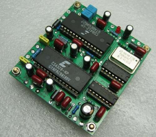
Why can't the hole be punched on the PCB pad? Many novices often encounter this problem when they first come into contact with printed circuit board. Because the board space is too small, device density resulting in small space, can not lead drilling, they usually choose to drill holes in the pad. Although this connection is a lot of convenience, but often it is not clear what kind of problems will lead to the board? Can you play it like this?
Why can't you make holes in the pad?
In early PCB designs, it was not allowed to have holes in the BGA pad. The main reason is to worry that tin leakage will lead to insufficient solder paste on the pad, which leads to the phenomenon of virtual welding and de-welding in the welding process of the device. Therefore, the general device punching is the first lead out and then punching.
At the present stage, due to the continuous reduction of BGA spacing, there will be no tin leakage through the resin plugging method, but the welding pad is drilled, there is a risk of welding or falling off, the cost will increase, and also affect the appearance of PCB board, so it is generally not recommended.
"Monument" phenomenon often occurs in CHIP components (such as patch capacitor, patch resistance) reflow welding process. The smaller the component size, the more likely it is to occur, such as 0201, 0402 and other small chip components. In the reflow welding process of surface mounting technology, SMD components appear to be warped until it leads to unwelding, because this situation is generally called "stellage" phenomenon.
The phenomenon of "standing tablet" is because the solder paste on the welding plate at both ends of the element is reflow melting, the surface tension of the two welding ends of the element is unbalanced, and the larger tension end pulls the element to rotate along the bottom of it. For some small packages of patch resistors and capacitors, it is best not to punch holes in the pad for the same reason. The hole is drilled at the edge of the pad, because the tension at both ends of the pad is inconsistent, prone to tombstone phenomenon.
Under what circumstances can a pad be perforated?
1, buried blind hole in general, when the BGA spacing is less than or equal to 0.5mm, BGA is not conducive to punching. In this case, blind burials can be used to solve the problem.
Blind hole: The blind hole is the through hole that connects the PCB inner wiring to the PCB surface wiring. The hole did not penetrate the entire PCB circuit board. Let's just go from the top layer to the middle third layer.
Buried holes: Buried holes are through-holes that only connect the lines between the inner layers, so they are not visible from the PCB surface.
Since the blind hole only penetrates the surface to the inner layer, rather than all the layers, no tin leakage occurs. The burrow is straight out of it, not to worry. The only problem is the cost. To sum up, the process and manufacturing cost of burying blind holes will be greatly increased.
2. Heat dissipation hole is very common in PCB design, in the recommended chip design, it is usually required to have a heat dissipation pad hole. In this case, the heat sink is used to dissipate the IC heat. Since there is no pin to be welded in the middle of the main body of the chip, there is no need to consider the problem of tin leakage and virtual welding on the IC heat dissipation pad through the hole.


Just upload Gerber files, BOM files and design files, and the KINGFORD team will provide a complete quotation within 24h.