
Professional PCB manufacturing and assembly
Building 6, Zone 3, Yuekang Road,Bao'an District, Shenzhen, China
+86-13410863085Mon.-Sat.08:00-20:00

Product overview specifications
Compared with most designs, PCB board performance requirements, cost, manufacturing technology and system complexity and other key factors have many conflicting requirements, PCB board laminated design is generally considered in various aspects of the key factors after a compromise decision. High - speed digital circuits and radio - frequency circuits are generally multilayer design.
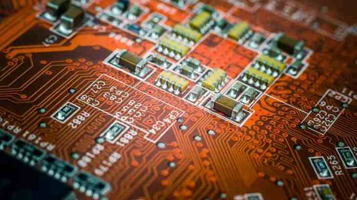
stratification
In a multilayer PCB board, there is usually a signal, power plane and ground plane. Generally speaking, the power plane and the ground plane are undivided solid planes. They will provide a good low-impedance current return path for signals that are in close proximity to each other.
Most of the signal layers are located between the power or ground reference plane layers, forming symmetrical or asymmetric strip lines. The top and bottom layers of multilayer PCB circuit boards are generally used to prevent components and a small amount of wiring. The wiring of such signals should not be too long, so as to reduce the direct radiation brought by the wiring.

Determine the single power reference plane
The use of decoupling capacitors is a crucial measure to deal with the integrity of power supply. Decoupling capacitors can only be stored at the top and bottom layers of the PCB.
The routing, pad and hole of the decoupling capacitor will seriously affect the effect of the decoupling capacitor. Therefore, in the design, the wiring connecting the decoupling capacitor must be fully considered, which should be as short and wide as possible, and the wire connecting to the hole should also be as short as possible.
Determine the multi-power reference plane
The multi-power reference plane will be divided into several solid regions with different voltages. If the signal layer is adjacent to the multiple power layers, the signal current on the nearby signal layer may encounter an unsatisfactory return path, resulting in gaps in the return path.
Compared with high-speed digital signals, these unreasonable return path design may cause serious problems, so high-speed digital signal wiring needs to be far away from the multi-power reference plane.
Determine multiple ground reference planes
Many ground reference planes can create one of the good low-impedance current return paths, which can greatly reduce common mode EMI.
The ground plane and the power plane need to be tightly coupled, and the signal layer needs to be tightly coupled to the adjacent reference plane. The thickness of the medium between layers is reduced to facilitate this purpose.
Rational design of wiring combination
The two levels across which a signal path crosses is a wiring combination. The best cabling combination design is to avoid flow of return current from one reference plane to another when possible. Instead, it is saved from one point (face) to another point (face) on one kind of reference plane.
In order to realize complex wiring, interlayer switching is inevitable. When transitioning between signal layers, ensure that the return current can flow smoothly from one reference plane to the other.
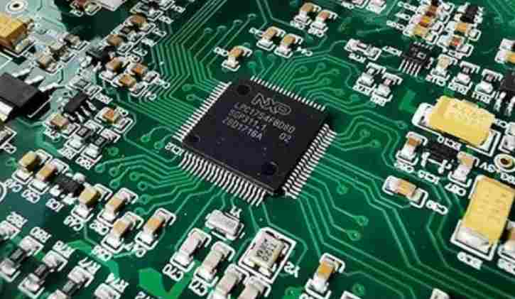
The circuit board makes the circuit miniaturized and intuitive, which plays an important role in the mass production of fixed circuit and the optimization of electrical appliance layout. The Circuit Board can be called Printed Circuit board or Printed circuit board, the English name is (Printed Circuit Board) PCB, (Flexible Printed Circuit board) FPC circuit board.
ROHS testing belongs to environmental protection testing, ROHS testing scope almost covers all electronic, electrical, medical, communications, toys, security information and other products, it not only includes the whole machine products, but also includes the parts used in the production of the whole machine, raw materials and packaging, related to the entire production chain. Circuit board export to the European Union is the need to do environmental protection ROHS testing, the following Xiaobian to introduce the circuit board ROHS testing.
ROHS ten test standard limits:
Pb lead 1000PPM
CD Cadmium 100PPM
Hg 1000PPM of mercury
Cr(VI) hexavalent chromium 1000PPM
PBBs polybrominated Biphenyl 1000PPM
PBDEs PBDES 1000PPM
DEHP Diethylhexyl phthalate 1000PPM
BBP Butyl benzyl phthalate 1000PPM
DBP Dibutyl phthalate 1000PPM
DIBP diisobutyl phthalate 1000PMM.
Circuit design What is pcb design software?
First, domestic use is protel, protel 99se, protel DXP, Altium, these are a company development, constantly upgrading software; The current version is Altium Designer 15 which is relatively simple and the design is more casual, but it is not very good to do complex PCBS these software.
Cadence spb This is Cadence software, the current version is Cadence spb 16.5; The ORCAD schematic design is the international standard; PCB design, simulation is very complete, use more complex than protel, mainly requirements, complex Settings; But for the design of the provisions, so the design of twice the result with half the effort, than protel is obviously strong.
3. BORDSTATIONG and EE of Mentor Company. BOARDSTATION is only applicable to UNIX system, not designed for PC, so few people use it. The current version of MentorEE is MentorEE 7.9 and Cadence spb, which belong to the same level of PCB design software. It is worse than cadence spb in some aspects. Its strengths are pulling wire and flying wire, so it is known as the king of flying wire.
EAGLE Layout This is the most widely used PCB design software in Europe. PCB design software mentioned above, used more, Cadence spb and MentorEE are worthy of the king. If you are a beginner in PCB design, I think Cadence spb is better. It can help designers develop a good design habit and ensure good design quality.


Just upload Gerber files, BOM files and design files, and the KINGFORD team will provide a complete quotation within 24h.