
Professional PCB manufacturing and assembly
Building 6, Zone 3, Yuekang Road,Bao'an District, Shenzhen, China
+86-13410863085Mon.-Sat.08:00-20:00


1. Problem 1: PCB board short circuit
This problem is one of the common faults that will directly cause the PCB board to fail to work, and there are many reasons for this problem, we will analyze one by one below.
The biggest cause for short circuit of PCB is improper design of welding pads. In this case, circular pads can be changed to oval pads to increase the distance between points to prevent short circuit.
Improper design of PCB parts direction will also cause the board short circuit, unable to work. Such as SOIC feet if parallel to the tin wave, it is easy to cause short circuit accident, at this time can be appropriate to modify the direction of the parts, so that it is perpendicular to the tin wave.
There is another possibility that will also cause PCB short circuit fault, that is the automatic plug-in foot bending. As IPC stipulates that the length of the pin is less than 2mm and the parts will fall off when the Angle of the foot is too large, it is easy to cause short circuit. It is necessary to leave the solder joint more than 2mm away from the line.
In addition to the three reasons mentioned above, there are also some reasons that will lead to the short circuit fault of PCB board, such as the hole of the substrate is too large, the temperature of the tin furnace is too low, the weldability of the board surface is poor, the failure of the welding resistance film, the pollution of the board surface, etc., are relatively common fault causes, engineers can compare the above reasons and the occurrence of faults one by one to eliminate and check.
2. Problem 2: Dark and granular contacts appear on the PCB board
PCB board dark or into small granular contact problem, mostly due to solder pollution and dissolved tin mixed with too much oxide, the formation of solder joint structure is too brittle. Care should be taken not to confuse the dark color with the use of low tin content solder.
Another reason for this problem is that the composition of the solder used in the process of processing and manufacturing changes, and the impurity content is too much. It is necessary to add pure tin or replace the solder. Physical changes in stained glass fibre-deposition, such as separation between layers. But this situation is not bad solder joint. The reason is that the substrate is heated too high, need to reduce the preheating and solder temperature or increase the substrate travel speed
3. Problem 3: PCB solder joints turn golden
In general, the solder of PCB board is silver gray, but occasionally there are golden solder joints. The main reason for this problem is that the temperature is too high. At this time, we only need to lower the temperature of the tin furnace.
Four, problem four: the bad board is also affected by the environment
Due to the structure of PCB itself, it is easy to cause damage to PCB board when in an unfavorable environment. Extreme temperature or temperature fluctuation, excessive humidity, high intensity vibration and other conditions are leading to board performance reduction or even scrap factors. For example, changes in ambient temperature can cause the board to deform. This will break the solder joints, bend the shape of the board, or it may cause the copper thread on the board to break.
On the other hand, moisture in the air can cause oxidation, corrosion and rust on metal surfaces, such as exposed copper wires, solder joints, pads and component leads. Accumulation of dirt, dust, or debris on the surface of components and circuit boards can also reduce air flow and cooling of components, leading to overheating and performance degradation of the PCB. Vibration, dropping, hitting or bending the PCB will deform it and cause the cracks to appear, while high current or overvoltage will cause the PCB board to be broken down or lead to the rapid aging of components and pathways.
5. Problem 5: PCB open circuit
An open circuit occurs when the trace breaks, or when the solder is only on the pad and not on the component lead. In this case, there is no adhesion or connection between the component and the PCB. Like short circuits, these can occur during production or welding and other operations. Vibrating or stretching circuit boards, dropping them, or other mechanical deformation factors can damage the trace or solder joints. Similarly, chemical or moisture can cause solder or metal parts to wear out, which can cause component leads to break.
6. Problem VI: Loosening or dislocation of components
During reflow soldering, widgets may float on the molten solder and eventually depart from the target solder joint. Possible causes of displacement or tilt include vibration or bouncing of components on welded PCB boards due to inadequate board support, reflux furnace setup, solder paste problems, human error, etc.
7. Problem 7: Welding problem
The following are some of the problems caused by poor welding practices:
Disturbed solder joint: The solder moves before setting due to external disturbance. This is similar to cold solder joints, but for different reasons, and can be corrected by reheating and ensuring that the solder joints are free from external interference while cooling.
Cold welding: This occurs when the solder does not melt properly, resulting in rough surfaces and unreliable connections. Cold solder spots can also occur as excess solder prevents full melting. The remedy is to reheat the joint and remove excess solder.
Solder Bridge: This happens when solder crosses and physically joins two leads together. These have the potential to form unexpected connections and short circuits that can cause components to burn out or burn out wiring if the current is too high.
Pad: Insufficient wetting of pins or leads. Too much or too little solder. A pad that has been raised by overheat or rough welding.

8. Question Eight: Human error
Most of the defects in PCB manufacturing are caused by human error. In most cases, faulty production processes, misplacement of components and unprofessional manufacturing specifications are responsible for up to 64% of avoidable product defects. The likelihood of defects increases with the complexity of the circuit and the number of manufacturing processes due to the following factors: densely packed components; Multiple circuit layers; Fine running of lines; Surface welded components; Power supply and ground.
Although every manufacturer or assembler hopes to produce a PCB board without defects, there are several design and production process problems caused by PCB board problems.
Typical problems and results include the following: poor welding can lead to short circuit, open circuit, cold welding spot, etc.; The misalignment of the plate layer will lead to poor contact and poor overall performance. Poor insulation of copper wire will lead to arc between copper wire and copper wire. Too close between the copper trace and the path, it is easy to short-circuit risk; The lack of thickness of the circuit board can lead to bending and breaking.

PCB layer design to follow the principles
Feb 09,2023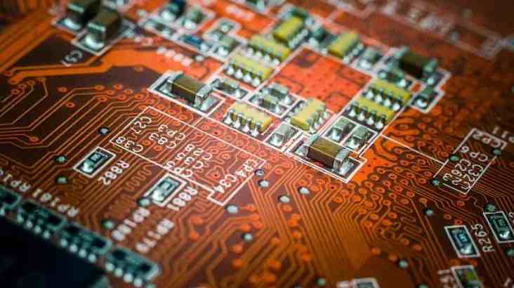


Just upload Gerber files, BOM files and design files, and the KINGFORD team will provide a complete quotation within 24h.