
Professional PCB manufacturing and assembly
Building 6, Zone 3, Yuekang Road,Bao'an District, Shenzhen, China
+86-13410863085Mon.-Sat.08:00-20:00

There are many aspects of PCB design that need to take into account the safe spacing. Here, it is temporarily classified into two categories: one is electrical related safety spacing, one is non-electrical related safety spacing.
Electrical related safety spacing
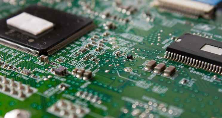
1. Distance between wires
As far as the processing capacity of mainstream PCB manufacturers is concerned, the spacing between conductors shall not be less than 4mil. Minimum line distance, also line to line, line to pad distance. From the perspective of production, the bigger the better if conditions exist, and the more common is 10mil.
2, pad aperture and pad width
As far as the processing capacity of mainstream PCB manufacturers is concerned, the aperture of pad shall not be less than 0.2 mm if drilled mechanically or 4mil if drilled with laser. The aperture tolerance varies slightly according to the different plates, which can generally be controlled within 0.05mm, and the minimum width of the pad shall not be less than 0.2mm.
3. Spacing between pad and pad
As far as the processing capacity of mainstream PCB manufacturers is concerned, the spacing between pad and pad shall not be less than 0.2 mm.
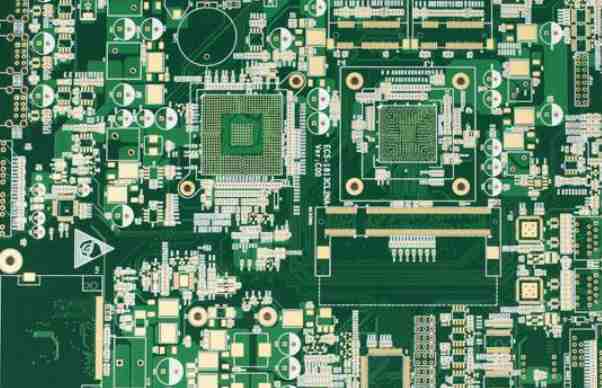
4, copper and plate edge spacing
The distance between live copper skin and PCB board edge should be no less than 0.3mm. Set the spacing rule on the Design-Rules-Board outline page.
If it is a large area of copper, there is usually a retraction distance with the edge of the plate, which is generally set to 20mil. In the PCB design and manufacturing industry, in general, for mechanical considerations of the finished circuit board, or to avoid the occurrence of curling or electrical short circuit caused by the exposure of copper skin on the edge of the board, engineers often shrink the large area of copper block relative to the edge of the board by 20mil, rather than laying the copper skin to the edge of the board.
There are many ways to deal with the indented copper, such as drawing a keepout layer on the edge of the plate and then setting the distance between the copper and the keepout. A simple method is described here, which is to set different safety distances for the copper objects. For example, the safety distance of the whole board is set to 10mil, and the safety distance of the copper is set to 20mil, which can achieve the effect of 20mil reduction in the edge of the board, and also remove the dead copper that may occur in the device.
Non-electrically relevant safety spacing
1. Character width, height and spacing
No changes can be made to the text film during processing, except that the width of the character lines below D-CODE less than 0.22mm (8.66mil) is enlarged to 0.22mm, that is, the character line width L = 0.22mm (8.66mil).
The width of the whole character W = 1.0mm, the height of the whole character H = 1.2mm, and the spacing between the characters D = 0.2mm. When the text is less than the above standard, the processing printing will be blurred.
2, through the hole to the hole spacing
Through hole (VIA) to through hole spacing (hole edge to hole edge) should be greater than 8mil.
3. Distance from screen printing to pad
Screen printing is not allowed to cover the pad. Because if the screen printing is covered with the pad, the screen printing will not be able to be tinned when tinning, thus affecting the installation of components. Generally, the board factory requires the spacing of 8mil to be reserved. If the PCB board is limited in area, the spacing of 4mil is barely acceptable. If the screen print is accidentally over the pad during the design, the plate factory will automatically eliminate the screen part left on the pad during manufacturing to ensure the tin on the pad.
Of course, in the design of the case by case analysis. Sometimes the screen printing is deliberately close to the pad, because when the two pads are very close, the middle screen printing can effectively prevent the short circuit of the solder connection during welding, which is another case.
4. 3D mechanical height and horizontal spacing
When installing PCB components, it is necessary to consider whether there will be conflicts with other mechanical structures in horizontal direction and spatial height. Therefore, in the design, it is necessary to fully consider the compatibility between components, PCB finished products and product shell and spatial structure, and reserve safe spacing for each target object to ensure that there is no conflict in space.
Earlier we discussed DFM and the importance of PCB design. So, what are the mainstream PCB design software? We are divided into free software, suitable for the design of low-end PCB board software, and suitable for the design of high-end PCB board software, roughly divided into three categories, to give you a brief introduction.
First, free software
1. ZentiPCB
ZentiPCB is a CAD based program that allows users to import netlist files and visualize their charts. The layout editor provides the ability to import components directly from the library using cursors, with support for single and dual panels depending on your requirements.
2. CometCAD
CometCAD electronic circuit schematic editor supports multi-page schematic, symbol rotation, part list and netlist schematic output. The PCB routing editor provides almost all of the functions mentioned earlier (component library, double-sided PCB, etc.), plus the ability to output CAM files and design rectangular multi-PCB boards.
3. Osmand PCB
Osmand PCB is a Mac-oriented PCB editor that can design wiring with spatial resolution as low as 10 nm and at arbitrary angles, and supports both imperial and metric units. Osmand also allows users to move and reposition components, connect/route/modify paths, and design PCB labels using the libraries they contain.
4. Design Spark
DesignSpark PCB provides schematic editing capabilities. Built on an integrated design environment, Designspark PCB provides all the tools you need to capture schematics and design and layout printed circuit boards (PCB) for free. Designspark PCB is a professional design tool.
5. Tiny CAD
TinyCAD offers the full functionality of PCB design and wiring design and contains 42 libraries with a total of 755 symbols, which include digital logic gate circuits, electromechanical components and even microcontrollers. Each component can be edited, and users can even add their own symbols to it. TinyCAD supports a variety of nettables (Eagle SCR, PADS-PCB, XML, etc.) and can also generate SPICE nettables.
Ii. Low-end
1. protel
Protel is relatively popular, and its market share far exceeds that of peer software. Many universities have protel courses, which are the basis for learning high-end PCB software.
protel has made great contribution to PCB design industry. Whether it is widely used Protel99 or subsequent versions, Protel provides an integrated design environment, including schematic design and PCB routing tools, integrated design document management, and support for collaborative design of workgroups through the network.
But while making a single panel with two layers works fine, after four, some versions start to feel unusable. In addition, Protel series software has higher requirements for system configuration, and the menu is too complicated, which is not suitable for high-speed PCB design.

2. power pcb
Powerpcb is a very popular low-end PCB design, easy to use, very easy to use, the quality of the board will not be inferior than wg, allegro, suitable for small and medium-sized enterprises.
3. or cad
The schematic design part of orcad, capture CIS, is regarded as one of the best schematic tools in the industry, with a nice interface, easy to use, easy to operate, and powerful simulation functions. However, the version of orcad is not so good, even worse than protel.
Iii. High-end
1. War gaming
The quality of cable is related to the quality of a PCB design software, and WG is a very good cable, its automatic wiring function is very powerful, wiring rules design is very professional.
2. en
EN is specially designed for large enterprises, it is difficult to learn, and there is no Chinese version, so it is not suitable for small and medium-sized enterprises. Both WG and EN are products of mentor, a graphic design software transformation that is rich in color and powerful in wiring.
3. allegro
Allegro is specialized in making large board, its rules are rigorous, powerful, automatic line, line repair, differential, multi-line and walk, repair copper skin and other functions, are very easy to use. But more difficult to get started, Chinese crack version is not much.
EMC considerations for PCB design
Feb 09,2023


Just upload Gerber files, BOM files and design files, and the KINGFORD team will provide a complete quotation within 24h.