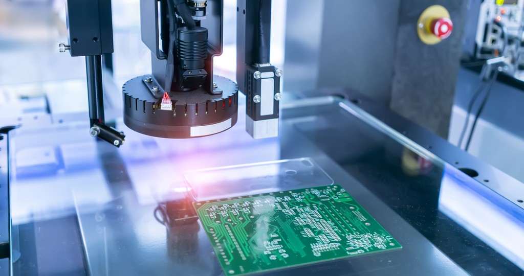
With the wide application of SMT surface mount technology, people have higher and higher requirements for SMT processing technology. SMT welding has a close relationship with all aspects of the entire assembly process, and once welding problems occur, product quality will be affected and loss will be caused.
1. Bridge Connection
Bridge connection refers to the solder misconnects two or more adjacent pads and contacts between the pads to form a conductive path. The causes of bridging are mostly caused by excessive solder or serious edge collapse after solder printing, or the size of the substrate welding area is out of line, SMD mounting offset, etc. In the stage of SOP and QFP circuits tending to micro-fine, bridging will cause electrical short circuit, affecting the use of products.
Preventive Measures:
1. The size of the substrate welding area should be set in accordance with the design requirements, and the SMD mounting position should be within the specified range.
2. To prevent the solder paste printing when the edge is bad, substrate wiring gap, solder resistance coating accuracy, must meet the requirements.
3. Formulate the appropriate welding process parameters to prevent the mechanical vibration of the welding machine conveyor belt.

Solder Ball
Solder ball refers to the solder forming scattered balls in unnecessary positions on the circuit board due to splashing and other reasons during the welding process. The production of solder balls is mostly caused by the rapid heating in the welding process and the solder flies, in addition, it is also related to the printing dislocation of the solder, the collapse of the edge, pollution and so on.
Preventive Measures:
1. Implement the corresponding preheating process according to the welding type.
2. according to the set temperature process for welding, to avoid welding heating in the excessive bad.
3. the use of solder paste should meet the requirements, no poor moisture absorption and other problems.
Cracks
When welded PCB is just out of the welding zone, due to the difference in thermal expansion of the solder and the part to be joined, under the action of rapid cooling or rapid heating, due to the influence of solidification stress or contraction stress, the SMD will produce micro-cracks. The welded PCB must also reduce the impact stress and bending stress on the SMD during punching and transportation.
Preventive Measures:
1. When designing surface mount products, it is necessary to take into account the gap between thermal expansion and correctly set heating and cooling conditions.
2. Choose good ductility solder.
Pull The Tip
Pinching refers to the appearance of a tip or burr in the solder joint. The reason is too much solder, less flux, heating time is too long, welding time is too long, the iron withdrawal Angle caused by improper.
Preventive Measures:
1. Choose the appropriate flux, control the amount of solder.
2. According to the PCB size, whether the multi-layer board, the number of components, there is no mounting components, etc. Set the preheating temperature.
Vertical Film Problem (Manhattan Phenomenon)
The Manhattan phenomenon refers to the phenomenon that one end of the rectangular chip element is welded to the pad, while the other end is tilted. The main reasons for this phenomenon are uneven heating at both ends of the component, unbalanced heating direction, welding paste melting and welding area size, SMD itself shape, wettability.
Preventive Measures:
1. Adopt a reasonable preheating method to achieve uniform heating during welding.
2. Reduce the surface tension on the SMD end when the solder melts.
3. The size of the substrate welding area length should be set appropriately, and the printing thickness size of the solder should be set correctly.
Poor Wetting
Poor wetting refers to the welding process of solder and substrate welding area, after wetting does not produce metal reaction, resulting in missed welding or less welding failure. Most of the reasons are caused by the contamination of the surface of the welding area, or by the solder resistance, or by the formation of a metal compound layer on the surface of the joint.
Preventive Measures
1. In addition to the implementation of appropriate welding techniques, anti-fouling measures should be taken on the surface of the substrate and the surface of the component.
2. Choose the appropriate solder, and set a reasonable welding temperature and time.
The above content is about the causes of poor welding and preventive measures for SMT patch processing, I believe you have some understanding. Because the process of SMT welding is more complicated, some welding problems can not be avoided in the work, we should learn to analyze the causes of each problem, and seek solutions, take preventive measures to reduce welding defects.


