
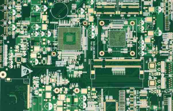
Professional PCB manufacturing and assembly
Building 6, Zone 3, Yuekang Road,Bao'an District, Shenzhen, China
+86-13410863085Mon.-Sat.08:00-20:00

Our electronic products are often more than 60% - reliability problems are in the PCB design of the electronic circuit board; Relevant theoretical and practical experience is required for working and performing PCBS; I often encounter various problems in product design practice; For example, the electronic circuit board cannot pass the EMS test standards, the problem of high frequency noise occurs when testing the functional pins of key devices IC, and the circuit functional IC pins detect interference noise for abnormal protection, etc.
By combining theory with practice; Test the difference between our theory and practice with test data! Good design and long-term experience is inseparable!
1. Switching power supplies share the general design principles through the following schematic diagram
We commonly use two kinds of switching power supply topology;
A. The area of main current return path in switching power supply topology is minimized. The drive pulse current loop is minimized.
B. For the isolated switching power supply topology, the current loop is separated by the transformer into two or more loops (primary side and secondary side), and the current loop should be designed separately with the minimum return area layout.
C. If the current loop has multiple ground points, the ground point should coincide with the central ground point.
D. In the actual design, we are constrained by conditions; If the capacitor of the 2 loops may not be good close to the common ground!
Key points of design:
We need to use electrical parallel approach to add a high-frequency capacitor to achieve common ground
2. PCB design ideas for non-isolated IC controller and main power loop system
As shown below - The unisolated power supply feeds the IC controller, which controls the load of the LED and performs dimming and other function control applications. The design of power supply and drive loop of the controller will affect the function and reliability of the system.
The wiring design through IC controller-PCB layout is as follows:
A1. The ground wiring of IC peripheral devices is preferentially routed and connected to IC-GND;
A2. IC-gnd connects to the grounding terminal of filter capacitor C1 (high frequency capacitor - low capacitance value), if the system is not isolated; When the main power system is working dynamically, no 12V non-isolated power supply is connected to the site.
A3. gnd of IC- control center should be single-point grounded! The C1 capacitor is near the IC-gnd pin, and the pin ground is connected to the C1 capacitor -gnd in the shortest way.
Critical loop
B. Minimum design principle of main power loop path
C. Topology current loop path minimization design principle
D. Pulse drive loop path minimization design principle
Note that when conditions are limited, the capacitors of the main circuit of the power supply and the topology circuit may not be in common, so we can use electrical parallel to add a high-frequency capacitor nearby to achieve common ground!
3. Specific BOOST LED driver architecture of PCB layout and wiring for specific analysis
The basic design idea is described above; Use the figure below for design analysis
In the illustration: The yellow jumper (JX) has a theoretical design with a 12V loop to minimize the loop area.
The highlighted blue part of the PCB is the GND cable routing. The highlighted white part is the positive cable routing of the 12-V IC power supply.
Verify the effect of yellow jumper (JX) grounding on the system through actual data testing:
Test conditions: 12-6A 115V / 600mA (light bar)
Test items: 12V load dynamic load interval 500ms max load/minimum load6.6A / 0.2A
Oscilloscope setup
CH1:12V (offset 10V) CH3:115V (offset 100V) CH4: ILED (offset 500mA)
Yellow jumper (JX) in the loop:
The dynamic response speed is increased by optimizing the loop response.
System loop effect of yellow jumper (JX) :
Because 12V provides VDD to the control IC at the same time, when the differential signal is routed, the 12V and GND wiring means that the backflow area between the power and ground is the minimum. When the 12V load is pulled, the 12V electrolytic capacitor is returning to the ground. When the 12V load current increases, the ground line impedance is not equal to 0, then there will be a voltage difference on the common ground impedance, resulting in the change of ground reference.

With the yellow jumper (JX) removed, the control loop becomes single-point grounded. In this case, the influence of ground potential reference is not affected by multiple circuit currents. Single point grounding in unisolated systems conforms to design theory.
Summary of design experience:
There may be multiple reasons. The IC power supply has multiple application functions.
A. For the isolated controller IC circuit, VDD is provided. When the differential signal is routed, the 12V and GND wiring means that the backflow area between the power and ground is minimum.
B. For GND of non-isolated IC control, avoid forming loops; The GND wiring of pins with the same function on the same side of IC should be connected together to IC-GND; The gnd of the IC- control center requires a single point grounding.
How to consider safe spacing in PCB design?
Feb 09,2023


Just upload Gerber files, BOM files and design files, and the KINGFORD team will provide a complete quotation within 24h.