
Professional PCB manufacturing and assembly
Building 6, Zone 3, Yuekang Road,Bao'an District, Shenzhen, China
+86-13410863085Mon.-Sat.08:00-20:00

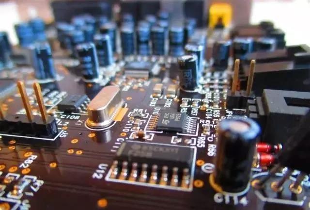
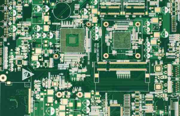
HDI, high density interconnected circuit board, is a kind of circuit board with relatively high circuit distribution density using micro blind buried hole technology. It contains an inner line and an outer line, and uses the drilling and the metallization process in the hole to realize the connection function between the internal layers of the line. And the most effective way to improve the density of PCB circuit board is to reduce the number of through holes, and precisely set blind holes, buried holes to achieve this requirement, and thus produced HDI buried blind holes plate. HDI buried blind hole board is one of the most precise PCB circuit boards, and its process is also the most complex. The core steps include the formation of high precision printed circuit, the processing of micro through hole and the plating of surface and hole.
1. Miniaturized HDI products
HDI miniaturization originally referred to the reduction in the size and weight of the finished product through its own wiring density design and the use of new high-density devices such as uBGAs. In most cases, the product's features have increased even as prices have held steady or fallen. The internal interconnect adopts the buried hole process structure mainly is 6 or 8 layer plate. HDI boards with high density substrates are mainly concentrated in 4 - or 6-layer boards. Interconnect the layers with buried holes, and at least two of the layers have microholes. It is designed to meet the increasing demand for high density I/O of flip chips. This technology will soon be integrated with HDI to enable miniaturization. The technology is suitable for flip chips or bonded substrates. The microporous process provides sufficient spacing for high density flip chips, even for 2+2 HDI products.
2. High level HDI products
High level HDI boards are usually traditional multilayer boards with laser drilling in layers 1 to 2 or layers 1 to 3. Using the necessary sequential lamination process, microporous machining on glass reinforced materials is another feature. The purpose of this technique is to reserve sufficient element space to ensure the required impedance level. The technology is suitable for high number HDI boards with high I/O numbers or fine-spaced components. The buried hole process is not a necessary process in this type of product. The purpose of the microhole process is only to form the spacing between high-density devices.
3. Ultra-fine line processing
With the development of science and technology, some high-tech equipment is becoming more and more miniaturized and refined, which requires more and more HDI board used. The line width/line distance of HDI boards for some devices has evolved from the early 5 mil (0.13 mm) to 3 mil (0.075 mm) and has become the mainstream standard. The higher and higher line width/line distance requirement brings the most direct challenge to the graphic imaging in PCB processing. So, how are the copper wires on these precision boards made? At present, the forming process of fine line includes laser imaging and pattern etching. Laser direct imaging (LDI) technology is to obtain fine circuit graphics directly by laser scanning on the surface of copper coated with photoresist. Laser imaging technology greatly simplifies the process flow and has become the mainstream technology in HDI PCB processing.
4. Microporous processing
The important feature of the HDI circuit board is that it has micro through holes (aperture ≤0.10 mm), which belong to the buried blind hole structure. At present, the buried blind holes on the HDI board are mainly processed by laser, but there are also CNC drilling. Compared with laser drilling, mechanical drilling also has its own advantages. When the epoxy glass cloth medium layer is processed by laser, the quality of the hole is slightly poor due to the difference in ablation rate between the glass fiber and the surrounding resin, and the residual glass fiber in the hole wall will affect the reliability of the through hole. Therefore, the advantage of mechanical drilling at this time is reflected. In order to improve the reliability and drilling efficiency of PCB board, laser drilling and mechanical drilling technology are steadily improved.
5. Electroplating and surface finishing
How to improve the plating uniformity and deep hole plating ability in PCB processing, improve the reliability of the board. This is dependent on the continuous improvement of electroplating process, from the ratio of electroplating solution, equipment deployment, operating procedures and other aspects. High frequency sound waves can speed up the etching ability; Permanganate solution can enhance the decontamination ability of the workpiece. The high frequency acoustic wave will stir and add a certain proportion of potassium permanganate electroplating solution in the electroplating tank. This helps the bath to flow evenly into the hole. Thus, the deposition capacity and uniformity of electroplating copper can be improved. At present, the copper plating for blind holes has been mature, and it can be used for through holes with different holes. The two-step copper plating method is suitable for different aperture and height-thick-diameter ratio of through holes. It has strong copper filling capacity and can reduce the thickness of surface copper layer as far as possible. There are many options for the final surface finish of PCB. Electroless nickel/gold plating (ENIG) and electroless nickel/palladium/gold plating (ENEPIG) are commonly used on high-end PCB board.


Just upload Gerber files, BOM files and design files, and the KINGFORD team will provide a complete quotation within 24h.