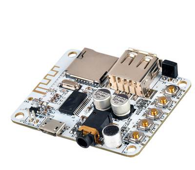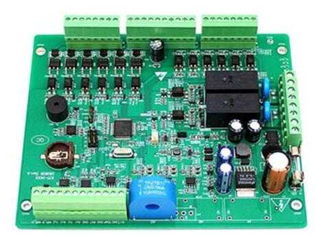
For non-electronic professional friends to see the wiring on the PCB circuit board, for high-speed signals, the line is not only connected from A to B so simple, but also to consider the "impedance factor", which will directly relate to whether the signal is complete from A to B point. Every time the engineers draw the PCB board, if there is a "do impedance" requirement for the PCB, they must attach the impedance requirement to the process requirements document (including what line, what value of impedance, control error, etc.).
Impedance requirements are proposed to ensure the integrity of high-speed signals on the circuit board, which plays a key factor in the normal and stable operation of high-speed digital systems. In high-speed systems, the key signal line cannot be regarded as an ordinary transmission line, and its characteristic impedance must be considered. If the impedance of the key transmission line is not matched, it may lead to signal reflection, rebound and loss. The original good signal waveform deformation (up flushing, down flushing, ringing phenomenon), it will directly affect the performance and even function of the circuit.
This is the same as the snake line. If you don't know about signal transmission, you can't understand why this line is not straightened directly. Isn't it the shortest line segment between two points? No, in electronic lines, especially high-speed signals, it is about matching, signal transmission is time, the longer the line, the longer the time is not the same, will affect the performance problems, of course, for low speed, these have no effect.
If the impedance does not match, then there will be a very large distortion and attenuation in the signal transmission process, and finally affect the function, light is unstable or transmission speed decreases, heavy direct strike direct function can not be achieved. The impedance values of different signals are not the same. The impedance of the difference line is generally 100 or 120 euros, such as high-speed USB and HDMI signals. The single-end impedance requirement is 50 euro 75 euro, etc. These requirements are the PCB engineer to determine the matter, PCB board factory according to your requirements, combined with their material PCB file circuit set, use impedance software tools to adjust, and finally use the equipment test, let it reach the required value.
So what are the factors that affect impedance?
It includes: line width, line distance, lamination, PCB board medium and thickness, which are all factors affecting impedance. Factory engineers adjust these values to meet the requirements. In practice, impedance is mainly controlled by controlling wire width and layering (because PCB substrate thickness is a fixed value, the more dynamic is the line width and line distance parameters).
Impedance line is divided into several types, different types, plate factory engineering in the software calculation of the object is not the same, here we should pay attention to. Therefore, it is necessary for PCB engineers to learn how to use PCB impedance calculation software to calculate whether the circuit currently designed meets the impedance value (the premise is to know that the board parameters used by the board factory can be more accurate).
1, according to the type of impedance line is divided into single-end impedance, differential impedance two types, said the popular point is for a single transmission line and a pair of difference lines. They are differential impedance, single-ended impedance, coplanar differential impedance, coplanar single-ended impedance:

2. The impedance line is divided into strip line and microstrip line according to the transmission medium.
Strip line: The wire in the medium between the two ground layers (or the power supply) of the signal line (the inner layer, with two reference planes) is divided into symmetrical strip line and asymmetric strip line according to the same or different distance between the transmission line and the two ground planes. The characteristic impedance of the strip wire is related to the thickness, width, dielectric constant and distance of the ground plane. There is a power supply or bottom layer on both sides of the strip, so the impedance is easy to control, while shielding is good.
Microstrip line: The transmission line separated from the ground (power) plane by electric medium (on the PCB surface, there is only one reference plane) is divided into two kinds of microstrip line, one is buried (inner layer), the other is unburied. The characteristic impedance of microstrip wire is determined by wire thickness, width, substrate thickness and dielectric constant. Mainly used for double layer and multi layer board.
1. Differential impedance
The reference ground plane is the same as the single-end impedance, the only difference is that the line width and line distance should also be adjusted
2. Characteristic impedance (single-end impedance)
For the impedance of many lines, only the bottom has a ground plane, refer to the closest stratum to do, if the line is the inner layer, refer to the closest two layers of ground plane to do.
3. Coplanar impedance (Coplanar difference and Coplanar characteristics)
Coplanar difference is surrounded by uniform copper, the distance between copper and impedance line is consistent, and there are rows of via holes on the copper, and there are ground planes under and around the coplanar difference impedance line.
4. Coplanar characteristics
(1) The function of impedance is to ensure the integrity of signal transmission, to ensure that the signal can be completely transmitted from point A to point B, without distortion.
(2) Impedance is mainly for high-speed signal requirements.
(3) Impedance values of different signals are different, which shall be confirmed by PCB design engineer combined with the requirements of the scheme.
(4) Impedance value is affected by many factors of PCB.
(5) Impedance value is calculated comprehensively through professional impedance calculation software, combining impedance type, line width, line distance, plate, laminated, plate thickness, medium and other factors.
(6) PCB board factory through equipment such as impedance tester test final impedance.
If there are a lot of key signals on the PCB to do impedance, you can attach a separate document, will be impedance control line display, and explain the value and error to do, circuit board factory will adjust the control of these "important signal" line. And the impedance value where does this information come from? Usually the chip specification manual, program requirements, or some industry all agree on a unified acceptance to the parameter value.


