
Professional PCB manufacturing and assembly
Building 6, Zone 3, Yuekang Road,Bao'an District, Shenzhen, China
+86-13410863085Mon.-Sat.08:00-20:00

kingford is a professional PCB design company with many years of working experience in PCB design team, which can undertake multi-layer, high density PCB design and PCB design proofing business. Next, we introduce how to consider welding technology in PCB design. How to consider welding technology in PCB design? In PCB design, the graphic design of power cord, ground wire and through-hole needs to consider the welding process from the following aspects. The following patch processing manufacturers to explain how to consider PCB design welding technology and how to maintain the advantages of PCBA processing enterprises related knowledge.
1. How do PCBA processing enterprises maintain their advantages
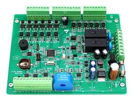
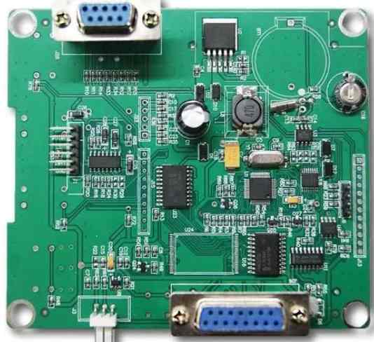
Shenzhen kingford Electronics professional to provide overall PCBA electronic manufacturing services, including upstream electronic components procurement to PCB production and processing, SMT patch, DIP plug-in, PCBA testing, finished product assembly and other one-stop services. Next, we will introduce how PCBA processing enterprises maintain competitive advantages. PCBA processing is the most important part of electronic products. The stability of PCBA processing quality directly affects the quality of electronic products. If PCBA processing can consistently maintain consistent quality and high productivity, the traditional manual processing mode will not work.
It has to rely on modern equipment. Brand new SMT machines now cost about 1.5 million yuan, and you need to buy 10-20 to build scale. Investment in equipment will shut out most "small workshop" businesses. In addition to more expensive SMT equipment and test equipment, PCBA processing requires significant working capital investment to improve material procurement systems and ensure storage of sensitive components. It is necessary to establish an anti-static storage room with constant temperature and humidity, which has strict requirements on the environment. If the manufacturing enterprise only through SMT to charge a low processing fee, then its development space and efficiency will be greatly compressed. At the same time, PCBA processing service objects are multinational companies, which often have a large business scale, which requires PCBA enterprises, as an important part of their global supply chain, must also have a large production scale.
Only by realizing large-scale production can we effectively reduce procurement cost and production cost. In order to become a large-scale branded supplier, PCBA processing plants should not only meet industry standards, but also pass the strict qualification certification of suppliers. International large enterprises should recognize the supplier qualification for at least one year, and put forward strict requirements on the supplier's production process, quality management, working environment, business conditions and other aspects during the approval process. Usually, they need to be corrected several times before they are certified, and then after a considerable period of testing for small quantities of supplies, they can officially become suppliers.
Once the manufacturer has passed the final review and approval of supplier qualification, it will be integrated into the global supply chain of the major international brands and can accept the purchase of its global production site. During this period, the comprehensive strength of the PCBA processing plant will be constantly evaluated. Only with a strong comprehensive strength and good service attitude of the PCBA processing plant will be recognized by large brands. PCBA processing industry needs to have a strong overall technical strength. Process technology, quality control level and production management techniques are very important, which often requires decades of practice and accumulation. At the same time, due to the rapid upgrade of electronic products, PCBA enterprises need to constantly update and improve for a long time.

2. How to consider welding technology in PCB design
1. Power line, ground wire: Because the thermal expansion coefficient and thermal conductivity rate of copper foil and substrate material on PCB are very different, so in preheating and welding temperature, the uneven distribution of copper foil layer is easy to cause large deformation and warping of PCB. Therefore, the following requirements should be met in PCB design: (1) The power line and ground wire of a large area should be drawn as a cross section line; (2) The distribution of copper foil patterns on each layer should be as uniform as possible.
2. Through hole (through hole) : The main function of the through hole (through hole) is to realize the electrical interconnection between PCB layers. Due to the large increase of PCB installation density, PCB multilayer development has been very common, so the role of the through hole (through hole) is more and more important, the number is also increasing. The layout and requirements of the through-hole (through-hole) in PCB design are as follows:
(1) The conduction hole shall be set away from the installation of the welding pad ≧0.63mm, and the conduction hole shall not be set in the welding pad area to avoid the loss of solder in the welding process;
(2) Try to avoid setting the pilot hole under the SMC/SMD component body to prevent the loss of solder and the retention of flux and dirt in the welding process, which cannot be removed;
(3) When the through-hole is connected to the power line or ground wire, for thermal isolation consideration, a thin neck wire with a width of not more than 0.25mm should be used for connection, and the length of the thin neck wire should be ≥0.5mm, or a thermal isolation ring should be used, as shown in the figure. The highest signal design rate: 10Gbps CML differential signal; Maximum number of PCB design layers: 40; Minimum line width: 2.4mil; Minimum line spacing: 2.4mil; Minimum BGA PIN spacing: 0.4mm; Minimum mechanical hole diameter: 6mil; Minimum laser drilling diameter: 4mil; Maximum number of pins:; 63000+ Max number of components: 3600; Maximum number of BGA: 48+. kingford PCB design service process 1. The customer provides schematic diagram to consult PCB design; 2. Evaluate quotation according to schematic diagram and customer design requirements; 3. The customer confirms the quotation, signs the contract and pays the project deposit; 4. Received advance payment and arranged engineer design; 5. After the design is completed, provide the screenshot of the document to the customer for confirmation; 6. The customer confirmed OK, settled the balance, and provided PCB designmaterials.


Just upload Gerber files, BOM files and design files, and the KINGFORD team will provide a complete quotation within 24h.