

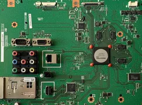
PCB design company introduces PCB design code layout rules
Considering the performance and processing efficiency of PCB, the preferred process sequence is as f...

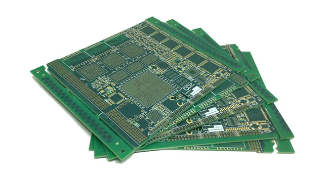
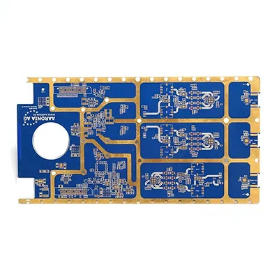
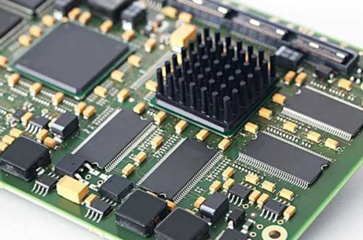
Kingford focus on the high-quality PCBA order demand of "Multiple varieties, medium and small batch, and short lead time".

Considering the performance and processing efficiency of PCB, the preferred process sequence is as f...
The PCB process design requirements are introduced in detail: 1, test point addition, 2, optical loc...
Common pads are: 1, square pad, 2, round pad, 3, island pad, 4, polygonal pad, 5, oval pad, 6, open ...
We should not only master various maintenance methods and analysis methods, but also learn and use t...
PCB design impedance matching: PCB design impedance matching refers to a suitable collocation betwee...

What inspection should be done before SMT patch processing: first, SMT patch components inspection, ...

First, clean the cured photosensitive film on the PCB. It is then cleaned of excess copper foil cove...
Note for circuit board welding: 1, after getting the PCB bare board, first check the appearance; 2, ...
Polygon filling deviation usually occurs when polygon plating copper on multi-grid circuit boards. W...
Circuit board design required data: 1. Circuit diagram, necessary, 2. Circuit consumption power calc...
The key points to understand the patch factory: 1. Professional cooperation, 2. Quality management p...
PCB board depends on science and technology, naturally must not lag behind, so the layout of high fr...