
Professional PCB manufacturing and assembly
Building 6, Zone 3, Yuekang Road,Bao'an District, Shenzhen, China
+86-13410863085Mon.-Sat.08:00-20:00

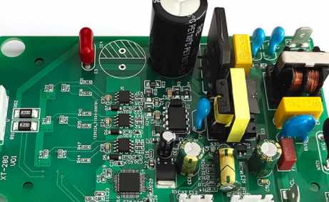
Shenzhen kingford own SMT plant, can provide minimum package 0201 components SMT processing services, support materials processing, OEM and other forms of processing. Next, I would like to introduce to you what inspection needs to be done before SMT patch processing.
I. SMT patch component inspection
The main test items of the components include: weldability, pin coplanar and serviceability, which should be sampled by the inspection department. The weldability of components can be tested by holding the components with stainless steel tweezers and dipping them into a tin pot at 235±5℃ or 230±5℃, and taking them out at 2±0.2s or 3±0.5s. Check the solder end under a 20-fold microscope, and the solder end of components should be more than 90% tin.
SMT patch processing workshop can do the following appearance inspection:
1. Visually or with a magnifying glass, check whether the welding end or pin surface of the component is oxidized or has any pollutants.
2. The nominal values, specifications, models, accuracy and dimensions of the components shall be consistent with the technical requirements of the products.
3. The pins of SOT and SOIC cannot be deformed. For the multi-lead QFP devices with lead spacing less than 0.65mm, the coplanicity of the pins should be less than 0.1mm(which can be detected by the optical mounting machine).
4. For products required to be cleaned by SMT patch processing, the marking of components shall not fall off after cleaning, and the performance and reliability of components shall not be affected (visual inspection after cleaning).
Two, printed circuit board (PCB) inspection
1. PCB solder pad graphics and dimensions, solder resistance film, screen, through hole Settings should meet the design requirements of smt printed circuit board. (For example: check whether the welding distance is reasonable, whether the screen is printed on the pad, whether the passthrough hole is done on the pad, etc.).
2. The overall size of PCB should be consistent, and the overall size, positioning hole and reference mark of PCB should meet the requirements of production line equipment.
3. Permissible warping size of PCB:
1) Upward/convex surface: maximum length 0.2mm/5Omm maximum length 0.5mm/ length direction of the whole PCB.
2) Downward/concave: maximum length 0.2mm/5Omm maximum length 1.5mm/ length direction of the whole PCB.
4. Check whether the PCB is contaminated or damp.

Three, SMT patch processing matters needing attention
1. SMT technician shall wear the electrostatic ring that has been verified to be OK, and check the electronic components of each order for no errors, mixing, damage, deformation, scratches and other undesirable phenomena before plug-in.
2. Prepare the electronic materials for the plug-in board of the circuit board in advance, and pay attention to the correct polarity direction of the capacitor.
3. After the completion of smt printing, check the defective products without missing insert, reverse insert, dislocation, etc., and transfer the good tinning finished products to the next process.
4. Before SMT patch processing and assembly, please wear electrostatic ring, keep metal sheet close to wrist skin and well grounded, and work alternately with both hands.
5. USB/IF seat/shield cover/high frequency head/network port terminal and other metal components, plug-in must wear finger cover operation.
picture
6. The position and direction of the inserted components shall be correct, the components shall be flat on the board surface, and the height components shall be inserted into the position of pin K.
7. If any material is found inconsistent with the specifications in SOP and BOM, report to the team leader in time.
8. Materials should be handled with care. Do not drop PCB boards that have gone through the early smt process and cause component damage.
9. Clean your work surface before going to and from work and keep it clean.
10. Strictly abide by the operation rules of the operation area. Products in the first test area, waiting area, defective area, maintenance area and less material area are strictly prohibited to be placed arbitrarily.
2. Why do PCB boards need to make plug holes?
Why do PCB board plug holes? In order to meet customer requirements, the circuit board must be plugged through the hole Via hole, after a lot of practice, change the traditional aluminum sheet plug process, with white mesh to complete the circuit board surface welding and plug holes, stable production, reliable quality.
The Via hole plays the role of connecting the lines to each other. The development of the electronics industry also promotes the development of PCB, which also puts forward higher requirements for PCB manufacturing process and SMT processing technology. Via hole plugging technology comes into being and should meet the following requirements:
1. Copper can be found in the through hole, and welding resistance can be plugged or not plugged;
2. Through the hole must have tin lead, there is a certain thickness requirements (4 microns), no solder ink into the hole, resulting in the hole hidden tin beads;
3. The pass-through hole must have solder resistance ink plug hole, light proof, no tin ring, tin beads and flat requirements.
With the development of electronic products to the direction of "light, thin, short, small", PCB also to high density, high difficulty development, so there are a large number of SMT, BGA PCB, and customers require plug holes when pasting components, mainly has five functions:
1. Prevent short circuit caused by tin penetrating through the component surface from the passthrough hole during wave soldering of PCB; In particular, when we put the hole on the BGA pad, we must first do the plug hole, and then gold-plated treatment, to facilitate the welding of BGA.
2. Avoid flux residue in the pass hole;
3. After the completion of SMT processing and component assembly in the electronics factory, PCB should be vacuumed on the testing machine to form negative pressure:
4. Prevent the surface solder paste from flowing into the hole causing virtual welding, affecting the installation;
5. Prevent over wave soldering tin bead pop out, resulting in short circuit.
4. Why do you choose kingford for SMT processing?
1. Strength guarantee
▪SMT workshop: We have imported SMT machines and several sets of optical inspection equipment, with a daily output of 4 million. Each process is equipped with QC personnel, who can keep an eye on product quality.
▪DIP production line: We have two wave-soldering machines, among which there are more than 10 old employees who have worked for more than three years. The skilled workers can weld all kinds of plug-in materials.
2. Quality assurance, cost-effective
▪ High-end equipment can stick precision shaped parts, BGA, QFN, 0201 materials. Can also template patch, loose material hand.
▪ Sample and size batch can be produced, proofing from 800 yuan, batch 0.008 yuan/point, no start-up fee.
3. Rich experience in SMT and welding of electronic products, stable delivery
▪ Accumulated SMT SMT processing services for thousands of electronic enterprises, involving many kinds of automotive equipment and industrial control motherboard. The products are often exported to Europe and the United States, and the quality can be affirmed by new and old customers.
▪ On time delivery, normal 3-5 days after complete materials, small batch can also be expedited on the same day shipment.
4. Strong maintenance ability and perfect after-sales service
▪ Experienced maintenance engineers can repair all kinds of patch welding caused by bad products, to ensure the connection rate of each piece of circuit board.
▪ 24-hour customer service staff at any time response, the fastest speed to solve your order problems.
Where can PCBA patch processing be done?
Mar 16,2023


Just upload Gerber files, BOM files and design files, and the KINGFORD team will provide a complete quotation within 24h.