
Professional PCB manufacturing and assembly
Building 6, Zone 3, Yuekang Road,Bao'an District, Shenzhen, China
+86-13410863085Mon.-Sat.08:00-20:00

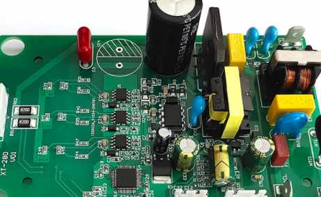
Shenzhen kingford is a PCB design company with many years of working experience in PCB design team, proficient in using mainstream PCB design software in the market, professional and efficient communication to ensure the progress of PCB design. Next, we introduce the role of matching resistance in PCB board design.
First, PCB design impedance matching
PCB design impedance matching refers to a suitable collocation between signal source or transmission line and load. According to the access mode PCB design impedance matching has serial and parallel two ways; According to the signal source frequency PCB design impedance matching can be divided into low frequency and high frequency two.
High frequency signals generally use serial PCB design impedance matching
The resistance value of the serial resistor ranges from 20 to 75Ω. The resistance value is directly proportional to the signal frequency and inversely proportional to the PCB wire width. In an embedded system, serial matching resistors are required for signals with a frequency greater than 20M and a PCB route length greater than 5cm, such as clock signals, data signals, and address bus signals in the system. Serial matching resistors serve two purposes:
1. Reduce high-frequency noise and edge overshoot. If the edge of a signal is very steep, it contains a large number of high frequency components, which will radiate interference, in addition, it is also prone to overshoot. The series resistance forms a RC circuit with the distributed capacitance of the signal line, the load input capacitance, etc., which reduces the steepness of the signal edge.
2. Reduce high-frequency reflection and self-excited oscillation. When the frequency of the signal is high, the wavelength of the signal is short. When the wavelength is short enough to match the length of the transmission line, the reflected signal superimposed on the original signal will change the shape of the original signal. If the characteristic impedance of the transmission line is not equal to the load impedance (that is, does not match), reflection will occur at the load end, resulting in self-excited oscillation. The low-frequency signals in PCB board can be directly connected, generally do not need to add serial matching resistance.
Parallel PCB design impedance matching is also called "terminal PCB design impedance matching".
Generally used in the input/output interface end, mainly refers to the PCB design impedance match with the transmission cable. For example, LVDS and RS422/485 use Class 5 twisted pair input matching resistance of 100~120Ω; The matching resistance of the video signal is 75 or 50Ω using coaxial cable and 300Ω using flat cable. The resistance value of parallel matching resistance is related to the medium of transmission cable, independent of the length, and its main function is to prevent signal reflection and reduce self-excited oscillation.
It is worth mentioning that PCB design impedance matching can improve the EMI performance of the system. In addition, in order to solve the problem of PCB design impedance matching, in addition to using series/parallel resistors, transformers CAN also be used to do impedance transformation, typical examples such as Ethernet interface, CAN bus, etc.

Two, zero ohm resistance
1. The simplest is to be used as a jumper. If a certain section of the line is not used, the resistance can be directly not welded (does not affect the appearance).
2. When the matching circuit parameters are uncertain, replace them with zero ohm. During the actual debugging, determine the parameters and replace them with components with specific values.
3. If you want to measure the working current of a certain part of the circuit, you can remove the zero ohm resistance and connect the ammeter, so as to measure the current conveniently.
4. In the PCB design and wiring, if the cloth is not past, you can also add a zero ohm resistance to play the role of crossover.
5. In high frequency signal network, acting as inductor or capacitor (PCB design impedance matching function, zero ohm resistance also has impedance). When acting as inductor, mainly to solve EMC problems.
6. Single point grounding, for example, analog ground and digital ground are connected to a single point common ground.
7. Configure circuits to replace jumpers and dip switches. Sometimes users will mess with the Settings, easy to cause misunderstanding, in order to reduce maintenance costs, the application of zero ohm resistance instead of jumper welding on the board.
8. System debugging, for example, the system is divided into several modules, and the power supply between modules is separated from the ground with zero ohm resistance. When the power supply or ground short circuit is found in the debugging phase, the zero ohm resistance can be removed to narrow the search range.
The above functions can also be replaced by "magnetic beads". Zero ohm resistance and magnetic bead although somewhat similar in function, but there are essential differences, the former is impedance characteristics, the latter is inductive characteristics. Magnetic beads are generally used in power and ground networks, and have filtering effects.
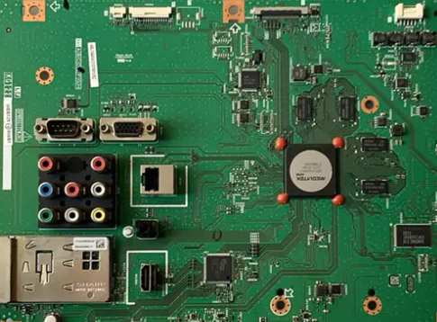
2 circuit board copying board proofing manufacturers
kingford is a circuit board copying and proofing manufacturer specializing in PCB copying and proofing, board copying and changing, chip decryption and backpushing schematic diagram services. It has its own PCB copying team and PCBA processing plant, which can realize rapid batch production of circuit board copying and proofing.
What is PCB copy board proofing?
Circuit board copy proofing refers to the design of the circuit board reverse technology research, also called cloning. In a narrow sense, copying board only refers to the process of extracting and restoring the PCB file of the electronic product circuit board and using the file to clone the circuit board; In a broad sense, copying board not only includes the extraction of circuit board files, circuit board cloning, circuit board imitation and other technical processes, And includes the modification of the circuit board file (that is, change the board), the three-dimensional data extraction and model imitation of the appearance mold of electronic products (that is, copy the number), the imitation of various electronic components on the circuit board, the decryption of the encrypted chip or single chip microcomputer on the circuit board, the disassembly of the system software of electronic products and other electronic products full set of cloning technology The process.
Circuit board copy proofing process
1. The customer shall provide the motherboard to be copied (prototype);
2. Copy PCB files, make BOM and reverse schematic diagram;
3. Produced PCB samples, purchased materials and processed welding according to board copying data;
4. The customer provides necessary debugging environment and prototype installation and commissioning;
5. The prototype is installed and adjusted, and the customer confirms the prototype.
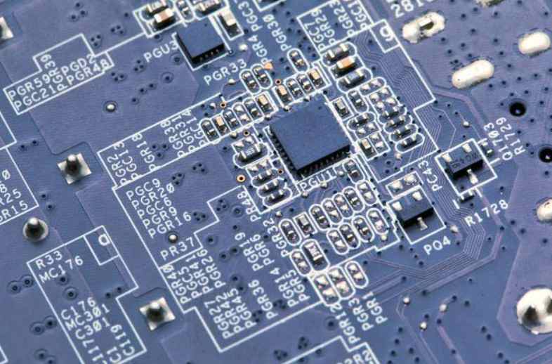
PCB design capability
Maximum signal design rate: 10Gbps CML differential signal;
Maximum number of PCB design layers: 40;
Minimum line width: 2.4mil;
Minimum line spacing: 2.4mil;
Minimum BGA PIN spacing: 0.4mm;
Minimum mechanical hole diameter: 6mil;
Minimum laser drilling diameter: 4mil;
Maximum number of pins:; 63000 +
Maximum number of components: 3600;
Maximum number of BGA: 48+.
PCB design service process
1. The customer provides schematic diagram to consult PCB design;
2. Evaluate quotation according to schematic diagram and customer design requirements;
3. The customer confirms the quotation, signs the contract and pays the project deposit;
4. Received advance payment and arranged engineer design;
5. After the design is completed, provide the screenshot of the document to the customer for confirmation;
6. The customer confirmed OK, settled the balance, and provided PCB design materials.


Just upload Gerber files, BOM files and design files, and the KINGFORD team will provide a complete quotation within 24h.