
Professional PCB manufacturing and assembly
Building 6, Zone 3, Yuekang Road,Bao'an District, Shenzhen, China
+86-13410863085Mon.-Sat.08:00-20:00

The rapid development of science and technology determines that all enterprises need to improve, among which PCB board depends on science and technology, naturally must not lag behind, so the layout of high frequency PCB has become the key point to be discussed when we design PCB high frequency board.
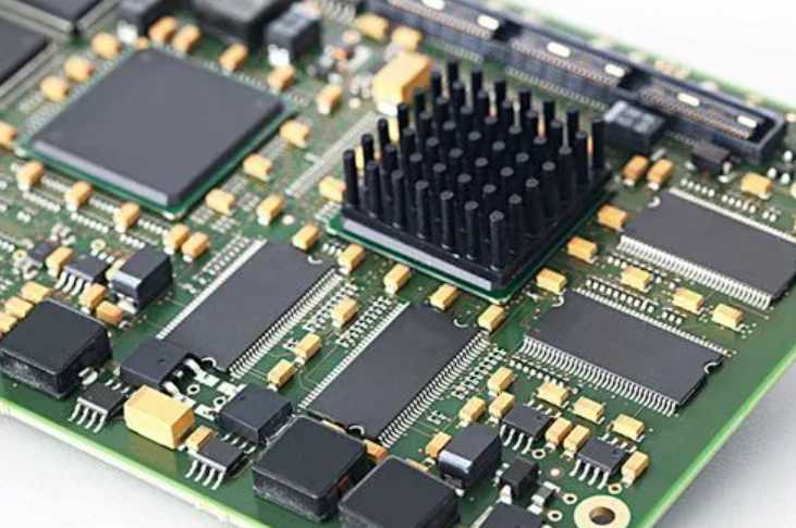
(1) High-frequency circuits tend to have high integration and high density wiring. The use of multilayer board is not only necessary for wiring, but also an effective means to reduce interference.
(2) The less lead bending between the pins of the high-speed circuit device, the better. The lead of high frequency circuit wiring is preferred to be solid line, which needs to be wound, and can be folded at 45° or circular fold. In order to meet this requirement, the external transmission and mutual coupling of high-frequency signals can be reduced.
(3) The shorter the lead between the pins of the high-frequency circuit device, the better.
(4) The less alternations between the wiring layers between the pins of the high-frequency circuit device, the better. By "minimizing layer crossing", we mean using as few through-holes (Via) as possible during component connection. It is estimated that one through-hole can bring a distributed capacitance of about 0.5 PF. The number of holes is reduced. Can greatly increase the speed.
(5) High frequency circuit wiring should pay attention to the "cross interference" introduced by parallel lines of signal lines. If parallel distribution cannot be avoided, a large area of "ground" can be placed on the back of parallel signal lines to greatly reduce interference. Parallel cabling in the same floor is almost inevitable, but in two adjacent floors, the direction of the cabling must be perpendicular to each other.
(6) Grounding measures surrounding particularly important signal lines or local units, i.e. drawing the outer outline of the selected object. Using this feature, so-called "packet" processing can be performed automatically on the selected important signal lines. Of course, for high-speed systems, it is also very beneficial to use this capability for local processing of components such as clocks.
(7) All types of signal wiring can not form a loop, and the ground wire can not form a current loop.
(8) A high-frequency decoupling capacitor shall be placed near each integrated circuit block.
(9) High-frequency turbulence links should be used when connecting analog and digital ground wires to common ground wires. In the actual assembly of high-frequency turbulent chains, high-frequency ferrite beads passing through the center hole are often used and are not usually represented in circuit schematics, and the resulting netlists do not include such components and wiring will ignore their presence. In response to this reality, it can be used as an inductor in a schematic, and the component package is defined separately in the PCB circuit board component library and manually moved to a suitable location near the convergence point of the common ground wire before wiring.
(10) The analog circuit and the digital circuit should be arranged separately. After independent wiring, the power supply and ground wire should be connected at one point to avoid interference with each other.
(11) Before connecting the DSP off-chip program memory and data memory to the power supply, the filter capacitor should be added and placed as close as possible to the chip power supply pin to filter out the power supply noise. In addition, it is recommended to mask around DSP and off chip program memory and data memory to reduce external interference.
(12) Off-chip program memory and data memory should be placed as close to the DSP chip as possible. At the same time, the layout should be reasonable so that the length of data lines and address lines are basically the same, especially when there are multiple memories in the system, the clock line of each memory should be considered. Clock input distance is equal, or a separate programmable clock driver chip can be added. For DSP system, the external memory with the same access speed as DSP should be selected. Otherwise, the high speed processing capability of DSP cannot be fully utilized. DSP instruction cycles are nanoseconds, so the most common problem in DSP hardware systems is high-frequency interference. Therefore, when making the printed circuit board (PCB) of DSP hardware system, special attention should be paid to the address line and data line. Signal cables should be connected correctly and reasonably. When connecting cables, make the high-frequency cables short and thick, and keep them away from easily interfered signal cables, such as analog signal cables. When the circuit around the DSP is more complex, it is recommended that the DSP and its clock circuit, reset circuit, off chip program memory and data memory form a minimum system to reduce interference.


Just upload Gerber files, BOM files and design files, and the KINGFORD team will provide a complete quotation within 24h.