
Professional PCB manufacturing and assembly
Building 6, Zone 3, Yuekang Road,Bao'an District, Shenzhen, China
+86-13410863085Mon.-Sat.08:00-20:00

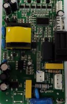
No matter the size and shape of the PCB designed, high-speed signal or low-speed signal, high-density multi-layer wiring or low-density single-layer wiring, there are always some common rules. Mastering these rules can greatly improve the efficiency of the drawing board, and also leave more room for improvement for the product design in the commissioning and finding out stage. The following Shenzhen PCB design company -kingford on these rules and rules summary and share for your reference.
First, plate frame drawing
1. Use 1mil (0.0254mm) line width when drawing the board frame;
2. The error between the outline size of the plate frame and the required assembly size is not more than 0.001mm;
3. The board frame is required to be chamfered (for safety regulations, depending on the product requirements), and the chamfered radius should be selected within 1~5mm. In special cases, refer to the structural design requirements.
2, the origin setting principle
The purpose is to ensure that the coordinates of the on-board SMT elements are in the first quadrant. In addition, the position of the origin can be selected as follows:
1. The intersection point of the left edge and the lower edge of the plate frame;
2. The positioning hole or screw hole in the lower left corner of the plate.

3, the forbidden area setting
1. Do not route cables or place components around the installation hole within 5mm diameter.
2. Special components shall set the forbidden area according to the specific requirements (or refer to the requirements of the product specification);
3. If there is no external working edge, do not wire or place components within 3mm of half edge.
4, the component placement level
The performance and processing efficiency of PCB board should be considered first. The optimal processing sequence is as follows:
1. If the component surface is mounted on one side: one reflow forming;
2. If the component surface patch and plug-in are mixed: one reflow welding, one wave welding molding;
3. Double-sided patch: two reflow welding molding;
4. Component surface patch and plug-in mixed assembly, welding surface assembly: two reflow welding, one wave welding molding;
5. Component surface patch and plug-in mixed assembly, welding surface is also patch and plug-in mixed assembly: two reflow welding, two wave welding molding, or one wave welding and one manual welding can also be.
5, the basic principles of layout operation
1. First place the installation holes, connectors and other components that need to be located, and set these components as immovable properties;
2. According to the layout principle of "big before small" and "difficult before easy", important unit circuits and core components should be laid out first;
3. Refer to the schematic diagram or schematic diagram, and arrange the main components according to the flow pattern of the main signals in the board;
4. Between high speed circuit and low speed circuit, between analog circuit and digital circuit, between high frequency circuit and low frequency circuit, between interference circuit and vulnerable to interference circuit should be fully isolated;
5. The same structure of the circuit, as far as possible to use "copy" standard layout;
6. Optimize the layout according to the standards of uniform distribution, balanced center of gravity and beautiful board surface.
Vi. Other details that need attention
1. Components of the same type shall be consistent in the direction of X or Y axis as far as possible;
2. The polar element of the same type should be consistent in the X axis or Y axis direction as far as possible;
3. The heating components should be evenly distributed to facilitate the heat dissipation of the veneer and the whole machine. The temperature sensitive components except the temperature detection components should be far away from the components with large heat dissipation;
4. The arrangement of components should be convenient for debugging and maintenance, that is, large components should not be placed around small components, and there should be enough space around the components to be debugged;
5. For the veneer produced by wave soldering process, the fastener mounting holes and positioning holes shall be nonmetallic holes. If the mounting holes need to be grounded, connect them to the ground plane by distributing ground holes as shown in the following figure.
6. When the patch element of the welding surface adopts wave soldering production process, the axial direction of the resistance container should be perpendicular to the direction of wave welding transmission, and the axial direction of the rejection and SOP (PIN spacing greater than or equal to 1.27mm) components should be parallel to the direction of transmission; IC, SOJ, PLCC, QFP and other active components with PIN spacing less than 1.27mm (50mil) should be avoided by wave soldering.
7. The distance between BGA and adjacent components shall be greater than 5mm, and the distance between other patch components shall be greater than 0.7mm. The distance between the outer side of the patch components and the outer side of the adjacent plug-in components shall be greater than 2mm.
8. The layout of IC peripheral decoupling capacitor should be as close to the IC power pin as possible, and make it form the shortest circuit between the power supply and the ground;
9. Component layout, should give due consideration to the use of the same power supply devices together as far as possible, in order to facilitate the division of the power supply area;
10. The layout of the container for impedance matching should be arranged reasonably according to its properties. The series matching resistors should be arranged close to the driver end of the signal, generally within 500mil. The layout of matching resistance and capacitor must distinguish between the source and the terminal of the signal, and match the terminal of multiple loads must be matched at the farthest end of the signal.
What is the cost of PCB design
Shenzhen kingford circuit board design capability
Maximum signal design rate: 10Gbps CML differential signal;
Maximum number of PCB design layers: 40;
Minimum line width: 2.4mil;
Minimum line spacing: 2.4mil;
Minimum BGA PIN spacing: 0.4mm;
Minimum mechanical hole diameter: 6mil;
Minimum laser drilling diameter: 4mil;
Maximum number of pins:; 63000 +
Maximum number of components: 3600;
Maximum number of BGA: 48+.
PCB design service process
1. The customer provides schematic diagram to consult PCB design;
2. Evaluate quotation according to schematic diagram and customer design requirements;
3. The customer confirms the quotation, signs the contract and pays the project deposit;
4. Received advance payment and arranged engineer design;
5. After the design is completed, provide the screenshot of the document to the customer for confirmation;
6. The customer confirmed OK, settled the balance, and provided PCB design materials.
What are the tips for PCB wiring?
Mar 17,2023


Just upload Gerber files, BOM files and design files, and the KINGFORD team will provide a complete quotation within 24h.