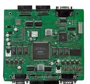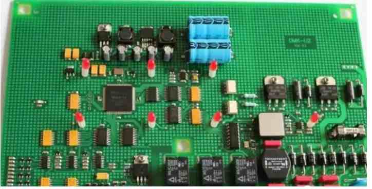
Why are the vast majority of PCB board colors green?
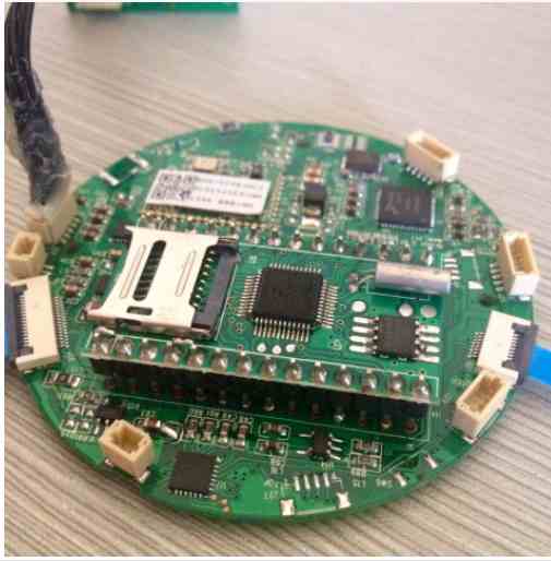
Actively promote the "PCB design - manufacturing - PCBA processing (SMT mount)" one-stop service model, with the goal of "creating the best overall value for the project", to eliminate the inconvenience of multi-party communication, fo...