
Professional PCB manufacturing and assembly
Building 6, Zone 3, Yuekang Road,Bao'an District, Shenzhen, China
+86-13410863085Mon.-Sat.08:00-20:00

The deformation causes of PCB board processing are very complex and can be divided into two kinds of stress caused by thermal stress and mechanical stress. The thermal stress is mainly generated in the process of pressing, and the mechanical stress is mainly generated in the process of stacking, handling and baking. The following is a brief discussion in the order of the process.

1.Copper coated incoming materials:
The copper clad plates are double panels, symmetrical structure, no graphics, copper foil and glass cloth CTE are almost the same, so there is almost no deformation caused by different CTE in the pressing process.
However, the large size of the copper-clad plate press and the temperature difference in different areas of the hot plate will lead to slight differences in the curing speed and degree of the resin in different areas during the pressing process, and the dynamic viscosity at different heating rates is also very different, so local stresses due to the differences in the curing process will also be generated.
Generally, this stress will maintain balance after pressing, but it will gradually release in the future processing to produce deformation.
2. Pressing:
PCB pressing process is the main process of generating thermal stress, similar to the copper clad plate pressing, will also produce local stress caused by the difference in the curing process, PCB board due to thicker thickness, diverse graphic distribution, more semi-cured sheets and other reasons, its thermal stress will be more difficult to eliminate than the copper clad plate.
The stress existing in the PCB board is released in the process of subsequent drilling, shape or barbecue, resulting in deformation of the board.
3. Welding resistance, character and other baking process:
Since the solder resistance inks cannot be stacked on each other when curing, the PCB board will be vertically placed in the shelf to dry the board for curing. The solder resistance temperature is about 150℃, which is just above the Tg point of the medium and low Tg material. The resin above the Tg point is highly elastic, and the board is easy to be deformed under the action of self-weight or strong wind of the oven.
4. Hot air solder leveling:
ordinary plate hot air solder the temperature of the tin furnace is 225℃~265℃, and the time is 3S-6S. The hot air temperature ranges from 280 ° C to 300 ° C.
The solder plate is fed into the tin furnace from room temperature, and then washed after treatment at room temperature within two minutes after being released. The whole hot-air solder leveling process is sudden heat quenching process.Due to the different materials and uneven structure of the circuit board, thermal stress will inevitably occur in the process of cooling and heating, resulting in microscopic strain and overall deformation warping.
5. Store:
The storage of PCB board in the semi-finished product stage is generally vertically inserted in the shelf, the tightness adjustment of the shelf is not suitable, or the stacking and placing of the board during the storage process will cause mechanical deformation of the board. In particular, the impact is more serious for thin plates below 2.0mm.
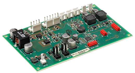
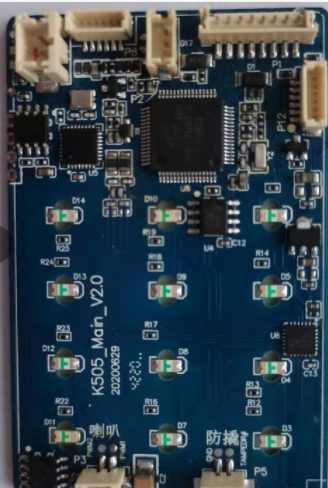
In addition to the above factors, there are many factors that affect the deformation of PCB board. Electronics is a professional manufacturer of printed circuit boards, 20 years of focus on single, double-sided, multi-layer circuit board production. Can provide FR4 hard board, FPC soft board, HDI board, metal substrate PCB proofing and mass production services.
PCBA proofing welding requirements
Jun 20,2023


Just upload Gerber files, BOM files and design files, and the KINGFORD team will provide a complete quotation within 24h.