
Professional PCB manufacturing and assembly
Building 6, Zone 3, Yuekang Road,Bao'an District, Shenzhen, China
+86-13410863085Mon.-Sat.08:00-20:00

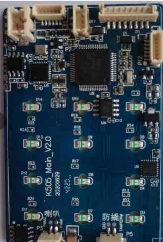
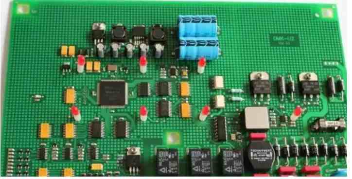
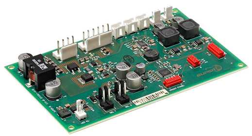
In PCB design, after completing the PCB design through many levels, the most important thing is the copyright issue, and plagiarism is common. So, how does PCB design prevent others from copying the board? Next PCB design company for you to introduce.
1, grinding, with fine sandpaper on the chip model wear off; It works better with a chip with a side door.
2, sealing glue, such as adhesive steel, etc., the PCB and its components are all covered; There are also five or six flying wires twisted together on purpose. It should be noted that the glue should not be corrosive, and the heat in the closed area is not too large.
")
3, the use of special encryption chips, such as ATMELAT88SC153.
4, the use of uncrackable chips, such as EPLD EPM7128 or above, ACTEL CPLD, etc.
5, use MASK IC, which requires a large batch.
6, the use of naked pieces, plagiars can not see the model and do not know the connection. But the chip's function is not too easy to guess.
7, the resistance above 60 ohms in series on the signal line with small current. (Ha ha, a bit bad, the premise can not affect the signal quality).
8, use some small components without words (or only some code) TO participate in signal processing, such as small patch capacitors, TO-XX diodes, etc.
9, PCB adopts buried hole and blind hole technology, so that the hole is hidden in the board. (A little expensive)
10, use other special accessories, such as customized LCD screen, customized transformer and so on.
11. Apply for a patent. In view of the poor environment of intellectual property protection, the best foreign method can only be put in the last in order to avoid production risks in advance, reduce unnecessary process costs, and reduce the project cycle, improve efficiency, the complex design detailed inspection and lengthy evaluation process are essential. The PCBA process inspection item rules cover all possible assembly problems, such as:
- Device analysis (component spacing, device to edge distance, component screen printing);
- Pin analysis (pin number difference, digit length, patch pin, through hole pin, press pin);
- Pad analysis (Chip pad spacing/length, pad connection, Mark number)
By checking the PCBA process project rules, you can solve a variety of production situations that engineers cannot anticipate in advance.
1. Component spacingAccurately detect pad spacing to avoid mutual interference
2. Device to edge Accurately detect the distance between the device and the edge of the board to avoid damaging the device during assembly.
3.Component screen printing
Accurately identify the characters related to the device to avoid the wrong components due to the character bit number error
4. Pin count difference
Accurately check the pin number of the pad to avoid causing the purchased components to fail to weld
5. Digit lengthCheck the bit length to avoid being unrecognized by the SMT machine
6. The patch pin accurately detects the area of the pad contact pin to avoid affecting the welding
7. Through hole pinAccurately detect the hole size and number of attributes of the through hole pin to avoid the purchase of components cannot be used
8. Press pinAccurately detect the hole size and number of attributes of the press pin, so as to avoid the failure of the purchased components to use the
9.Chip pad
Accurately detect the size of Chip pad to avoid bad welding
10. Pad connectionAccurately identify whether the pad is not connected, to avoid the problem of open circuit
11. Mark points accurately check whether there is a mark point in the board, the number of mark points, to avoid affecting the patch
12. Marker analysis
Accurate detection of objects around the mark point, whether it has an impact mark Point Identification Co., Ltd. specializes in providing overall PCBA electronic manufacturing services, including upstream electronic component procurement to PCB production and processing, SMT patches, DIP plug-ins, PCBA testing, finished product assembly and other one-stop services.
The company gives full play to its competitive advantages in scale procurement and quality control, and has signed long-term cooperation agreements with many electronic component manufacturers at home and abroad and around the world to ensure the quality and stable supply of raw materials, and transfer the benefits to customers.Long-term maintenance of IC, resistors, capacitors, inductors, audiodes and other components procurement advantages, can greatly save customers' inventory costs, improve production turnover efficiency, save time. Currently for the United States, Britain, Japan, Russia, France, Canada, Australia, Romania, Switzerland and other countries and regions to provide PCBA processing services.


Just upload Gerber files, BOM files and design files, and the KINGFORD team will provide a complete quotation within 24h.