
Professional PCB manufacturing and assembly
Building 6, Zone 3, Yuekang Road,Bao'an District, Shenzhen, China
+86-13410863085Mon.-Sat.08:00-20:00

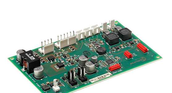
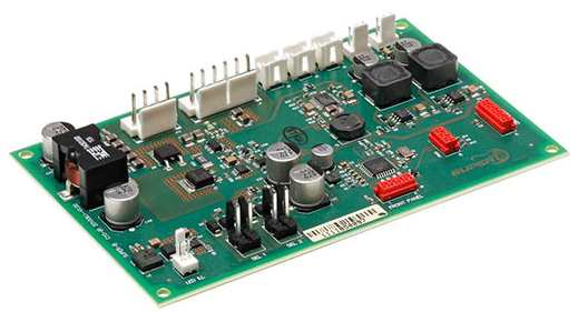
In PCBA processing, patch components and plug-in components are used. So what is the difference between patch components and plug-in components in PCBA processing? Next, PCBA processing manufacturer kinhford Electronics will introduce you.
First, the difference between the two:
1, the patch components are small in size, light in weight, and easier to weld than plug-in components.
2, the chip element has a very important advantage, that is, to improve the stability and reliability of the circuit; Because the patch element has no leads, the stray electric and magnetic fields are reduced, which is especially effective in high-frequency analog circuits and high-speed digital circuits.
")
Two, the welding method of the two
1, patch components welding method:
Put the component on the pad, apply the adjusted patch solder paste on the surface of the component and the contact point of the pad, and then heat the joint of the pad and the patch element with 20W internal heat electric soldering iron (the temperature should be 220~230℃), and remove the electric soldering iron after seeing the solder melt, and welding will be completed after the solder solidifies. After welding, you can clamp the welded patch component with tweezers to see if it is loose. If there is no loosening, it means that the welding is good. If there is loosening, you should re-apply the solder paste to re-weld according to the above method.
2, plug-in components welding method:
When soldering all pins, solder the tips of the iron and apply flux to all pins to keep them wet. Touch the end of each pin of the chip with the tip of the iron until the solder flows into the pin. After soldering all the pins, wet the pins with flux to clean the solder to eliminate any short circuits and lapping. Finally, use tweezers to check whether there is a spot weld, after the check is complete, remove the flux from the circuit board, dip the hard brush with alcohol along the direction of the pin carefully wipe until the flux disappears.
Electronics Co., Ltd. specializes in providing integrated PCBA electronic manufacturing services, including upstream electronic component procurement to PCB production and processing, SMT patches, DIP plug-ins, PCBA testing, finished product assembly and other one-stop services.
The company gives full play to its competitive advantages in scale procurement and quality control, and has signed long-term cooperation agreements with many electronic component manufacturers at home and abroad and around the world to ensure the quality and stable supply of raw materials, and transfer the benefits to customers.


Just upload Gerber files, BOM files and design files, and the KINGFORD team will provide a complete quotation within 24h.