SMT Small Batch SMT Processing Plant Before The Material Work
Special materials such as integrated circuits should be stored in anti-static drying cabinets, and special integrated circuits such as BGA should be baked before being placed.


Special materials such as integrated circuits should be stored in anti-static drying cabinets, and special integrated circuits such as BGA should be baked before being placed.
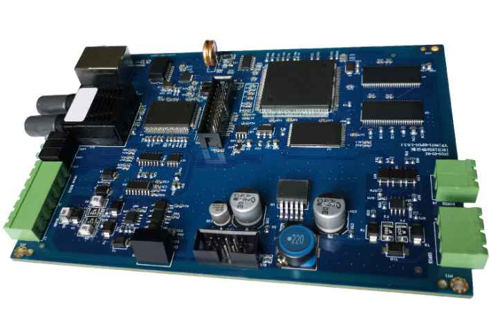
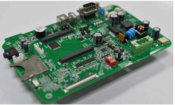
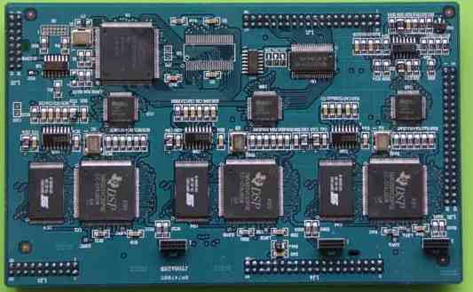
We provide PCBA processing services, starting from the production of PCB circuit boards, each production process has strict quality control.
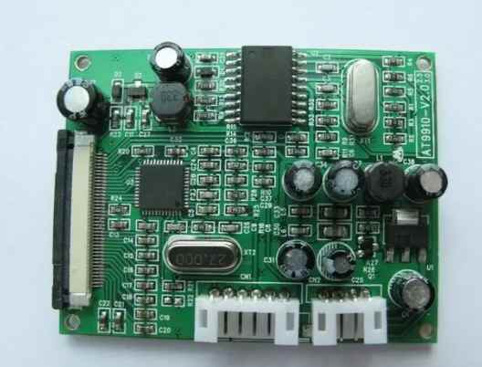
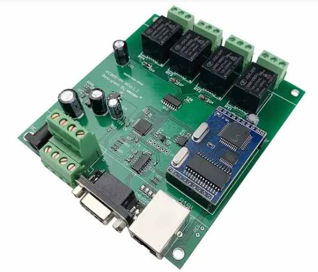
SMT processing plants play an important role in the electronics processing industry and are indispensable for the precision and miniaturization of electronic products.

Pcb circuit board proofing: pcb circuit board proofing refers to the production of a small part of the product as a sample before the start of mass production, so that it can be better completed, and the perfect combination of mass production circuit boar

As cars become more intelligent and electrified, automakers are increasing their demand for the quantity and precision of electronic components.

The high quality requirements of SMT chip processing require us to apply a clear work responsibility system, such as SMT chip processing related positions operators need to conduct professional training, and implement the first piece inspection
PCB board is composed of copper foil, resin, glass cloth and other materials. Each material has different physical and chemical properties. there will inevitably be residual thermal stress, which leads to deformation.
Review according to PCB checklist, including design rules, layer definition, line width, spacing, pad and hole Settings, focusing on the rationality of device layout.
The first layer in the middle is laid with multiple GND, several lines can be laid, but do not divide each layer of copper; The second layer of VCC copper in the middle has multiple power supplies laid separately. A small number of lines can be laid, but
In order to prevent deformation of many electronic products, the thickness of the board is left at 1.0mm, 0.8mm, or even 0.6mm.
Adopt shielding measures providing packet ground for high speed signal is an effective way to solve crosstalk problem.
Another version of the "3W" rule states that when using sawtooth wiring for lead length matching, the sawtooth width needs to be at least three times the width of the lead, which minimizes the discontinuity of the lead impedance


