
Professional PCB manufacturing and assembly
Building 6, Zone 3, Yuekang Road,Bao'an District, Shenzhen, China
+86-13410863085Mon.-Sat.08:00-20:00

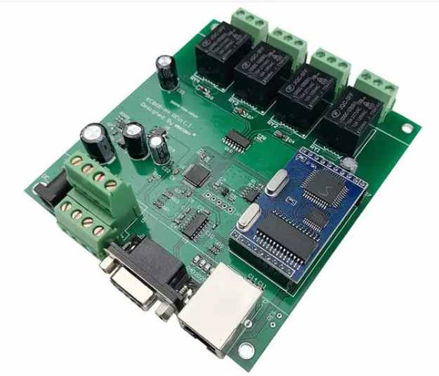
Multilayer PCB is the result of the development of electronic information technology to the direction of high speed, multi-function, large capacity, small volume, thin and lightweight. For the production of PCB boards, the more layers, the more programs are produced, the failure rate will increase correspondingly, and the corresponding cost will be higher. Therefore, multilayer boards are generally used in advanced circuits. Four-layer board is a common multi-layer PCB, so what are the four layers of four-layer boards?

The four layers of the PCB board are divided into: signal layer (top layer), signal layer (bottom layer), power layer (middle layer) and formation (middle layer). Usually, the component is placed on the top layer of the PCB, so the top layer is also called the component surface; The bottom layer is generally used for welding, so the bottom layer is also called the welding surface. For the patch component, the upper and lower layers can be placed components. Four-layer PCB board layout:
1. The first layer in the middle is laid with multiple GND, several lines can be laid, but do not divide each layer of copper; The second layer of VCC copper in the middle has multiple power supplies laid separately. A small number of lines can be laid, but do not divide each layer.
2. Wiring has four layers, generally the TOP LAYER, Buttom Layer, VCC and GND four layers. Generally, through holes, buried holes, blind holes and other ways are used to connect between layers, which is more than double-layer PCB boards. In addition, the VCC and GND layers should try not to use signal lines.
Shenzhen Kingford Technology Co., Ltd. is a circuit board manufacturer specializing in printed circuit board manufacturing, 20 years of focus on single, double sided, multi-layer circuit board production. Can provide FR4 hard board, FPC soft board, HDI board, metal substrate PCB proofing and mass production services.
To make a complete PCB, you need to go through many complex processes. If there are some operational errors in the PCB production process, it will lead to quality problems in the final finished board and do not meet the product requirements. The PCB wire break problem will affect the realization of PCB functions:
Common causes of PCB wire breakage
1. film process: film is not firm, bubbles appear. If the film is wet, there will be garbage contamination.
2. Exposure process: the negative film has problems caused by scratches or garbage, including exposure machine problems, insufficient exposure parts, etc.
3. Development process: Development is ambiguous.
4. Etching process: nozzle pressure is too high, etching time is too long. Electroplating problems: uneven plating or surface adsorption force. What is the cause of PCB board breakage? First of all, look at the form of broken wire, by analyzing the form of broken wire, find out the process of PCB board broken wire caused by the problem, and then gradually investigate the possible causes in the production process.
Shenzhen Kingford Technology Co., Ltd. is a circuit board manufacturer specializing in printed circuit board manufacturing, 20 years of focus on single, double sided, multi-layer circuit board production. Can provide FR4 hard board, FPC soft board, HDI board, metal substrate PCB proofing and mass production services.


Just upload Gerber files, BOM files and design files, and the KINGFORD team will provide a complete quotation within 24h.