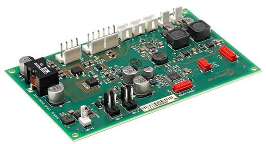
Pcb circuit board proofing: pcb circuit board proofing refers to the production of a small part of the product as a sample before the start of mass production, so that it can be better completed, and the perfect combination of mass production circuit boards and actual functional requirements. pcb proofing has the following specific process:
The first step: First of all, we need to tell the manufacturer the relevant data of the size, process requirements, product quantity and so on, and then there will be professionals for you to quote, place orders and follow up the production situation.
Step 2: According to the requirements of the customer, on the board that meets the requirements, cut off small pieces of production board that need to meet the requirements, the specific process is as follows: large board → cutting board according to the MI requirements → curium board → beer round edge grinding → board out.
The 3: The main operation is to drill holes according to the customer's information, drill out the size of the hole in the appropriate position, the specific process is as follows: stack pin → upper plate → drilling → lower plate → inspection and repair.
Step 4: The main operation is copper sinking. The principle of copper sinking is to deposit a thin layer of copper on the insulation hole by chemical method. The specific process is as follows: rough grinding → hanging plate → automatic copper sinking line → lower plate → dipping 1% dilute H2SO4→ thickening copper.

Step 5: This operation is the graphics transfer, which refers to the transfer of the graphics on the production film to the large board. The specific process is as follows: hemp plate → film pressing → static → alignment → exposure → static → impact → inspection.
Step 6: Graphic plating is to electroplate a copper layer of the required thickness and a gold-nickel or tin layer of the required thickness on the exposed copper skin or hole wall of the line pattern, the specific process is as follows: upper plate → oil removal → water washing twice → micro-corrosion → water washing → pickling → copper plating → water washing → acid plating → tin plating → water washing → lower plate.
Step 7: This operation is mainly to use NaOH solution to remove the anti-plating coating layer to expose the non-line copper layer.
Step 8 : The etching process, the main operation is to use the chemical reagent copper reaction, so that you can remove the non-line parts.
Step 9 : The process of green oil, which transfers the green oil film graphics to the board, and its main role is to protect the line and prevent the role of tin on the line when welding parts.
Step 10 : Mainly printed some characters on the circuit board, the printing of characters is mainly the information of some manufacturers. The specific process is as follows: green oil final curium → cooling static → adjusting screen → printing characters → after curium.
Step 11: Gold-plated finger, plated a layer of nickel gold required thickness on the plug finger, so that it has more hardness and wear resistance
Twelfth: molding; Through the mold stamping or CNC gong machine gong out the customer needs the shape forming method organic gong, beer plate, gong, hand cutting.
Step 12: Circuit board test: mainly through the electronic 100% test, detect the circuit board visual is not easy to find open circuit, short circuit and other defects affecting functionality and other related problems.
PCB Surface Spray Tin Treatment Advantages And Disadvantages
After the PCB board is produced, some surface treatment will be carried out, and Pate Technology will introduce you to the advantages and disadvantages of the treatment method of HASL.
HASL is the main lead surface treatment process used in industry. The process is formed by immersing the board in a lead-tin alloy, and excess solder is removed by a "wind knife", which is a hot air blowing on the surface of the board. For PCA production
Process, HASL has many advantages: it is the cheapest PCB, and the surface layer can be welded after many reflow, cleaning and storage.
For ICT, HASL also offers a process for solder auto-covering test pads and holes. However, HASL surfaces have poor flatness or coplanarity compared to existing alternatives. There are now several lead-free HASL replacement processes, which are becoming more and more popular due to the natural substitution properties of HASL. HASL has worked well for many years, but with the advent of "eco-friendly" green process requirements, the days of this process are numbered. In addition to lead-free problems, increasing board complexity and finer spacing have exposed many limitations to the HASL process.
Advantages: Lowest cost PCB surface process, maintaining weldability throughout the manufacturing process, with no negative impact on ICT.
Disadvantages: Lead-based processes are commonly used, which are now restricted and will eventually be eliminated by 2007. For fine pin spacing (< 0.64mm), which can cause solder bridging and thickness problems. Uneven surfaces can lead to coplanarity problems in the assembly process.
Shenzhen Kingford Technology Co., Ltd. to give you the best quality SMT chip processing, PCB production, embedded system research and development, electronic processing, embedded motherboard,PCBA contract materials services.


