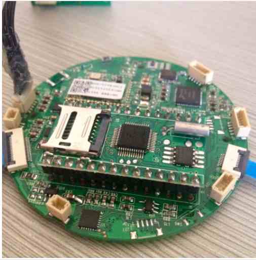
1,The outer frame (clamping edge) of the PCB assembly should adopt a closed-loop design to ensure that the PCB assembly will not be deformed after it is fixed on the fixture;
2, PCB board width ≤260mm(SIEMENS line) or ≤300mm(FUJI line); If automatic dispensing is required, PCB board width × length ≤125 mm×180 mm;
3, PCB assembly shape as close to the square, recommended to use 2×2, 3×3,...... A jointed board; But don't put it together as a yin-yang board;
4, the center distance between the plates is controlled between 75 mm and 145 mm;
5. When setting the reference anchor point, an open weld area larger than 1.5 mm is usually set aside around the anchor point;
6. There can be no large devices or protruding devices near the connection point between the outer frame and the internal small board, the small board and the small board, and the edge of the components and the PCB board should be left with a space greater than 0.5mm to ensure the normal operation of the cutting tool;

7, four positioning holes are opened at the four corners of the outer frame of the plate, the aperture is 4mm±0.01mm; The strength of the hole should be moderate to ensure that it will not break during the process of upper and lower plates; The aperture and position accuracy should be high, the hole wall is smooth without burrs;
8, each small board in the PCB assembly must have at least three positioning holes, 3≤ aperture ≤6 mm, no wiring or placement is allowed within 1mm edge positioning holes;
9, for the whole board positioning of PCB and the reference symbol for the positioning of fine-pitch devices, in principle, the QFP with a spacing of less than 0.65mm should be set in its diagonal position; The positioning reference symbols for the PCB sub-board should be used in pairs and arranged diagonally on the positioning elements;
10, large components should have positioning columns or positioning holes, such as I/O interface, microphone, battery interface, microswitch, headphone interface, motor, etc.;
PCB layout and PCB design specifications
1. Layout design specifications.
A. The distance from the edge of the plate should be greater than 5mm =197mil.
B. First place the components closely related to the structure, such as connectors, switches, power sockets, etc.
C. Prioritize the core components of the circuit function block and the larger components, and then place the surrounding circuit components with the core components as the center.
D, high-power components are placed in a position conducive to heat dissipation.
E, the larger quality components should avoid being placed in the center of the board, should be placed near the fixed side of the chassis.
F, the components with high-frequency connections are as close as possible to reduce the distribution of high-frequency signals and electromagnetic interference.
G, input, output components as far away as possible.
H, with high pressure components as far as possible in the debugging hand is not easy to reach the place.
I, the thermal element should be far away from the heating element.
J, the layout of adjustable components should be easy to adjust.
K, consider the signal flow direction, and rationally arrange the layout to keep the signal flow direction as consistent as possible.
L, the layout should be uniform, neat and compact.
M, SMT components should pay attention to the direction of the pad as much as possible, in order to facilitate welding, reduce the possibility of bridging.
N, the decoupling capacitor should be near the power input end.
O, the height of the wave soldering surface is limited to 4mm.
P, for the PCB circuit board with components on both sides, the larger and denser IC, the plug-in components are placed on the top layer of the board, and the bottom layer can only put smaller components and a small number of pins and loosely arranged patch components.
Q, it is particularly important to add heat sinks to small-size high-heat components, high-power components can be dissipated by applying copper, and try not to put heat sensitive components around these components.
R, high-speed components as close as possible to the connector; The digital circuit and the analog circuit are separated as far as possible, it is best to separate the ground, and then a single point ground.
S, the distance between the positioning hole and the nearby pad is not less than 7.62mm(300mil), the distance between the positioning hole and the edge of the surface attachment device is not less than 5.08mm(200mil).
2. Wiring design specifications
A, the line should avoid acute angles, right angles, should use 45 degrees of line.
B. Signal lines on adjacent layers are orthogonal.
C, high-frequency signal as short as possible.
D, input, output signals as far as possible to avoid adjacent parallel wiring, it is best to add ground wire between the lines to prevent feedback coupling
E, dual panel power cord, the direction of the ground wire is best consistent with the data flow to enhance the anti-noise ability
F, digital, analog to separate.Clock line and high frequency signal line should consider the line width according to the characteristic impedance requirements to achieve impedance matching.
G, the whole circuit board wiring, drilling to be uniform.
H, separate power layer and formation, power line, ground as short and thick as possible, power and ground formed by the loop as small as possible.
I, the clock wiring should be less holes, try to avoid and other signal lines and walk the line, and should be far away from the general signal line, to avoid interference with the signal line; At the same time, avoid the power supply part on the board to prevent the power supply and the clock from interfering with each other; When there are multiple clocks of different frequencies on a circuit board, two clock lines of different frequencies cannot run parallel. The clock line is kept away from the output interface to prevent the high-frequency clock from coupling to the output CABLE line and being emitted; If there is a special clock generator chip on the board, the line can not be traced below it, copper should be laid under it, and the special land should be cut off if necessary;
J, pairs of differential signal lines are generally parallel lines, as little as possible through the hole, must punch holes, should be two lines together to achieve impedance matching.
K, the distance between the two solder joints is very small, the solder joints shall not be directly connected; The hole leading from the pad should be as far away from the pad as possible.


