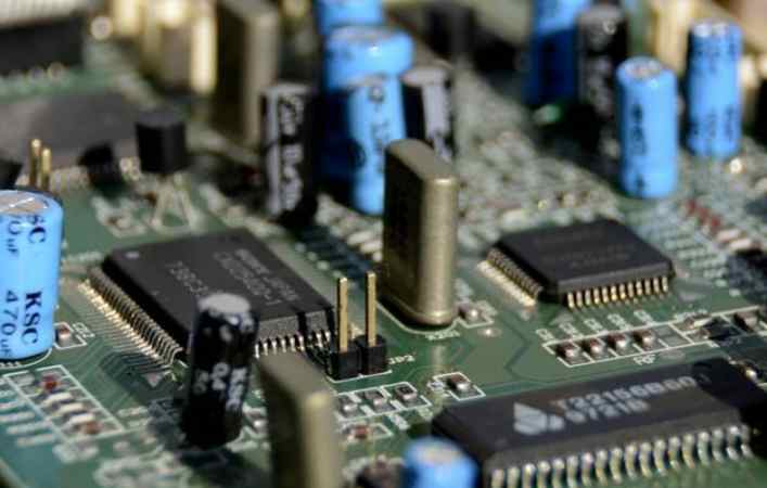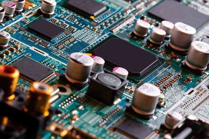
The harm of finger contact PCB is briefly introduced
Therefore, staff should develop the habit of wearing gloves, which can reduce the harm of direct contact with pcb board. The following is a brief introduction of a hand printing will lead to bad pcb board reasons, hazards, and how to avoid.