
Professional PCB manufacturing and assembly
Building 6, Zone 3, Yuekang Road,Bao'an District, Shenzhen, China
+86-13410863085Mon.-Sat.08:00-20:00

PCB board technology, including computer aided manufacturing processing technology, namely CAD/CAM, as well as light painting technology. The following is an introduction to computer aided manufacturing processing technology
Computer aided manufacturing (CAM) is a kind of process processing according to the specified process. All the technical requirements mentioned above should be prepared before light painting. Such as mirroring, solder expansion, process line, process frame, line width adjustment, center hole, contour line and other issues should be in
CAM this process to complete. In particular, it should be noted that the spacing between user files is too small, must be dealt with accordingly. Because each factory's process flow and technical level are different, in order to meet the user's final requirements, must make necessary adjustments in the production process, in order to meet the user has
Close precision and other aspects of the requirements. So CAM processing is an essential process in modern printed circuit manufacturing.
The work done by CAM
Modification of the size of the welding disk, combined with D code.
The correction of the width of the line, combined with D code.
⒊ Inspection of minimum spacing, between pad and pad, between pad and line, and between line and line.
A check of the aperture size has been made of it.
The minimum line width of the inspection.
It confirmed the expansion parameters of solder resistance.
It is mirrored.
Add various craft lines, craft box.
⒐ for modified lateral erosion line width correction.
⒑ form center hole.
⒒ add horn line shape.
⒓ and locating holes.
⒔ puzzle, rotate, mirror.
⒕ spell.
⒖ graphic overlay processing, cutting Angle tangent handle.
Trademark ⒗ add users.
Organization of CAM process
As there are dozens of popular CAD software on the market, so the management of CAD process must first start from the organization, a good organization will achieve the effect of twice the result with half the effort.
Gerber data format has become the standard of light painting industry, so Gerber data should be taken as the object of processing in the whole light painting process. The following problems arise if CAD data is used as an object.
⒈ There are too many types of CAD software. If various process requirements must be completed in CAD software, each operator must be skilled in the operation of each CAD software. This will require a long training period before the operator can become skilled enough to meet the actual production requirements.
This is both time - and economically unjustifiable.
Because of the various requirements of the process, some requirements for some CAD software is impossible to achieve. Because CAD software is used for design, it does not take into account the special requirements in the process, so it cannot meet all the requirements. And CAM software is specifically used for process processing,
Doing these jobs is the best.
⒊CAM software is powerful, but all the Getber file operation, and not the CAD file operation.
If it is processed by CAD, it is required that every operator be equipped with all CAD software, and there are different process requirements for each CAD software. This will create unnecessary confusion for administration.
In summary, a CAM organization should have the following structure (especially for medium and large sized enterprises).
(1) All process processing uniformly takes Gerber data as the processing object.
(2) Each operator must master the skills of converting CAD data into Gerber data.
(3) Each operator shall master one or more methods of operating CAM software.
(4) Develop a unified process specification for Gerber data files.
CAM processes can be handled relatively centrally by several operators for easy management. Reasonable organization will greatly improve management efficiency, production efficiency, and effectively reduce the error rate, so as to achieve the effect of improving product quality.
Test method:
Needle bed method
This method consists of a probe with a spring attached to each detection point on the circuit board. The spring gives each probe a pressure of 100-200g to ensure good contact at each test point. The probes are arranged together in such a way that they are called "needle beds". Under the control of the detection software, the detection points and signals can be programmed. Figure 14-3 is a typical structure of a needle bed tester, and the tester can know the information of all the test points. The probes are actually installed only for the test points that need to be tested. Although it is possible to inspect both sides of the board at the same time using the needle bed test method, it is advisable to design the board so that all inspection points are on the welded side of the board. Needle bed tester equipment is expensive and difficult to maintain. Different arrangements of needles are selected according to their specific application.
A basic general-purpose grid processor consists of a drilled board with pins with center spacing of 100, 75, or 50mil. The pins act as probes and make direct mechanical connections using electrical connectors or nodes on the circuit board. If the pad on the circuit board matches the test grid, the polyvinegar film, perforated to specification, is placed between the grid and the circuit board to facilitate the design of a specific probe. Continuity detection is achieved by accessing the end point of the grid, which has been defined as the x-y coordinates of the pad. Since every network on the circuit board is checked for continuity. Thus, an independent test is completed. However, the proximity of the probes limits the effectiveness of the needle-bed method.

observation
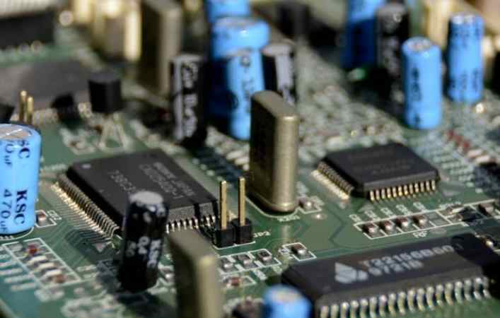
Circuit board is small in size and complex in structure, so the observation of circuit board must use professional observation instruments. Generally, portable video microscopes are used to observe the structure of the circuit board. Through video microcameras, the microscopic structure of the circuit board can be clearly seen from the microscope. In this way, it is easier for us to design and test the circuit board. The portable video microscope is used in the factory site, the portable video microscope MSA200, VT101, because it can realize "observation at any time, at any time to detect, many people discuss" more convenient than the traditional microscope!
Flying needle test
The flying needle tester does not rely on a pin pattern mounted on the fixture or bracket. Based on this system, two or more probes are mounted on tiny freely moving magnetic heads in the x-y plane, and the test points are directly controlled by CADI Gerber data. The two probes can move within 4mil of each other. The probes can move independently, and there is no real limit to how close they are to each other. A tester with two arms that move back and forth is based on the measurement of capacitance. The circuit board is pressed against an insulating layer placed on a sheet of metal to act as another sheet of metal for the capacitor. If there is a short circuit between the lines, the capacitance will be larger than at a certain point. If there is a break, the capacitance will be smaller.
Test speed is an important standard for choosing a tester. The needle-bed tester can accurately test thousands of test points at a time, while the flying needle tester can only test two or four test points at a time. In addition, a single-side test with a needle-bed tester may only cost 20-305, depending on the complexity of the board, while a fly needle tester may require Ih or more to complete the same evaluation. Shipley (1991) explained that even though manufacturers of high volume printed circuit boards find moving fly pin testing techniques slow, this method is a good choice for manufacturers of complex circuit boards in lower volumes.
For bare board testing, there are special testing instruments (Lea,1990). A more cost-effective approach would be to use a generic instrument, which, although initially more expensive than a dedicated instrument, would be offset by a reduction in the cost of individual configurations. For general purpose grids, the standard grids for boards and surface mount devices with pin components are 2.5mm. At this time the test pad should be greater than or equal to 1.3mm. For Imm grids, test pads are designed to be larger than 0.7mm. If the grid is small, the test needle is small, brittle, and easily damaged. Therefore, it is best to choose a grid larger than 2.5mm. Crum (1994b) states that the combination of a universal tester (a standard grid tester) and a flying needle tester can make the detection of high-density circuit boards both accurate and economical. Another method he suggests is to use a conductive rubber tester, a technique that can be used to detect points that deviate from the grid. However, the different height of the pad with hot air leveling will hinder the connection of the test point.
The following three levels of detection are usually performed:
1) Bare plate detection;
2) Online detection;
3) Function detection.
The universal tester can be used to detect a type of circuit board, and it can also be used to detect special applications.

Must PCB circuit board do impedance?
Feb 04,2023


Just upload Gerber files, BOM files and design files, and the KINGFORD team will provide a complete quotation within 24h.