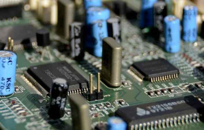
With the introduction of surface mount technology, automatic detection technology of circuit board is applied, and the packaging density of circuit board increases rapidly. Therefore, even for the density is not high, the general number of circuit board, circuit board automatic detection is not only basic, but also economical. In complex circuit board inspection, two common methods are the needle bed test and the double probe or fly needle test.
Detector:
According to the characteristics of the material of the circuit board and a wide range of applications, in order to more effectively save volume and achieve a certain accuracy, so that the characteristics of three degrees of space and thin thickness better applied to digital products, mobile phones and laptops. Recommended for circuit board (FPC) testing instruments are MUMA200 all-aluminum alloy optical image measuring instrument, three-axis automatic optical image measuring instrument VMC250S, VMC four-axis automatic optical image measuring instrument, VMS series optical image measuring instrument and so on.
Working level:
The circuit board includes many types of working layers, such as signal layer, protective layer, screen layer, internal layer, etc. The functions of various layers are briefly described as follows:
⑴ Signal layer: mainly used to place components or wiring. Protel DXP usually contains 30 intermediate layers, namely Mid Layer1~Mid Layer30. The middle layer is used to lay out signal lines, and the top layer and the bottom layer are used to place components or apply copper.
(2)The protective layer: mainly used to ensure that the board does not need tin plating place is not tinned, so as to ensure the reliability of the board operation. Top Paste and Bottom Paste are the top solder resistance layer and the bottom solder resistance layer respectively. Top Solder and Bottom Solder are solder protection layer and bottom solder, respectively.
(3) Screen printing layer: mainly used to print the serial number of components on the circuit board, production number, company name, etc.
⑷ Internal layer: mainly used as the signal wiring layer, Protel DXP contains 16 internal layers.
⑸ Other layers: Mainly includes 4 types of layers.
Drill Guide: Mainly used for drill position on PCB.
Keep-Out Layer: Mainly used to draw the electrical frame of the circuit board.
Drill Drawing: Mainly used for setting drill shape.
Multi-Layer: Mainly used to set the multi-layer.
Design process:
⒈ The basic design process of the circuit board can be divided into the following four steps:
⑴ Design of circuit schematic diagram
Circuit schematic design is mainly to use the schematic editor of Protel DXP to draw schematic diagram.
⑵ Generate a network report
The network report is the report showing the link between the circuit principle and each component, it is the bridge and link connecting the circuit diagram design and circuit board design (PCB design), through the network report of the circuit diagram, you can quickly find the connection between the components, so as to provide convenience for the later PCB design.
⑶ The design of printed circuit board
The design of printed circuit board is usually referred to as PCB design, which is the final form of circuit schematic transformation. The related design of this part is more difficult than that of circuit schematic design. We can use the powerful design function of Protel DXP to complete the design of this part.
(4) Generate printed circuit board statements
After the design of the printed circuit board is completed, various reports need to be generated, such as the generation of pin report, circuit board information report, network state report, and finally printed circuit diagram.

The design of circuit schematic diagram is the basis of the whole circuit design, its design directly determines the effect of PCB design. Generally speaking, the circuit schematic design process can be divided into the following seven steps:
⑴ Start the Protel DXP schematic editor
⑵ Set the size and layout of the circuit schematic diagram
(3) Take out the required components from the component library and place them on the working plane
(4) Connect components according to the design
⑸ Adjust the components after wiring
⑹ Save the schematics document that has been drawn
⑺ Print out the drawing
⒊ The drawing size, direction and color are mainly achieved in the Documents Options dialog box. Execute the Design→Options command to open the Documents Options dialog box and set the drawing size in the Standard styles area. A4 to OrCADE paper type can be selected from the drop-down list box. Set the Orientation of the drawing through the orientation option in the Options section of the "Documents Options" dialog box. Click the button and select Landscape to set the horizontal drawing. Select Portrait and set the vertical drawing. The setting of the drawing Color can be realized in the Options section of the drawing setting dialog box. Click the Border Color block to set the drawing border color, and click the Sheet Color block to set the drawing background color.
By running the Design→Options→Change System Font command, the "Font" dialog box appears. Through the dialog box, users can set the system font, the color, size, and the font used by the system font.
4. The grid and cursor are mainly implemented in the "Preferences" dialog box. To open the "Preferences" dialog box, run Tools→Preferences.
Set the grid: In the Preferences dialog box that opens, select the Graphical Editing TAB. In the Visible Grids section of the Cursor Grid Options section, select Line Grid to set the line grids. Select the Dot Grid option for a point grid (no grid).
Setting the Cursor: Select the Cursor Type option of Cursor Grid Options in the Graphical Editing TAB. There are three cursor types under this option: Large Cursor90, Small Cursor90, and Small Cursor45. The user can select any of the cursor types.


