
Professional PCB manufacturing and assembly
Building 6, Zone 3, Yuekang Road,Bao'an District, Shenzhen, China
+86-13410863085Mon.-Sat.08:00-20:00

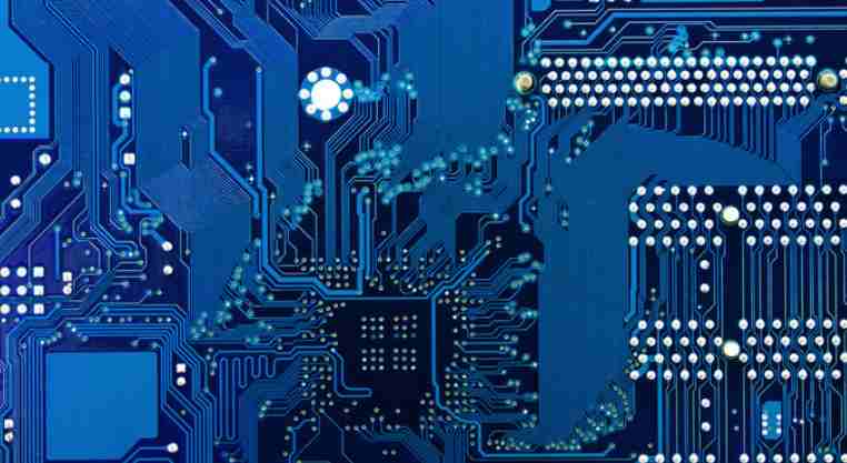
Circuit board names are: ceramic circuit board, alumina ceramic circuit board, aluminum nitride ceramic circuit board, circuit board, PCB board, aluminum substrate, high frequency board, thick copper plate, impedance board, PCB, ultra-thin circuit board, ultra-thin circuit board, printing (copper etching technology) circuit board, etc. The circuit board makes the circuit miniaturized and intuitive, which plays an important role in the mass production of fixed circuit and the optimization of electrical appliance layout. Circuit boards may be called printed circuit boards or printed circuit boards, English name is (Printed Circuit Board) PCB, (Flexible Printed Circuit board) FPC circuit board (FPC circuit board also known as flexible circuit board Flexible circuit board is made of polyimide or polyester film as a base material with high reliability, Excellent flexible printed circuit board. It has the characteristics of high wiring density, light weight, thin thickness and good bending. and Soft and hard combination plate (reechas, soft and hard combination plate) - the birth and development of FPC and PCB, gave birth to the soft and hard combination plate this new product. Therefore, the combination of soft and hard board, is the flexible circuit board and hard circuit board, after pressing and other processes, according to the relevant process requirements combined together, the formation of a circuit board with FPC characteristics and PCB characteristics.
Classification:
Circuit boards according to the number of layers to be divided into single panel, double panel, and multilayer circuit boards three big classification.
The first is the single panel. On the most basic PCB, the parts are concentrated on one side and the wires on the other. This type of PCB is called a single-sided circuit board because the wires appear on only one side. Single panels are usually simple and inexpensive to make, but the disadvantage is that they cannot be used on complex products.
Dual panel is an extension of single panel, when single-layer wiring can not meet the needs of electronic products, dual panel will be used. Both sides are covered with copper and have a route, and the line between the two layers can be guided through the hole, so that it forms the required network connection.
The multilayer board refers to a printed board having more than three layers of conductive graphics layers and insulating materials between them, and the conductive graphics between them are interconnected according to requirements. Multilayer circuit board is electronic information technology to high speed, multi-function, large capacity, small volume, thin, lightweight direction of development products.

According to the characteristics of the circuit board to be divided into soft board (FPC), hard board (PCB), soft and hard combined board (FPCB). [1]
Circuit board board:
FR-1: Flame retardant copper clad phenolic paper laminate. IPC4101 Detail Specification Number 02; Tg N/A;
FR-4:1) Flame retardant copper clad epoxy E glass fiber cloth laminates and bonded sheet materials. IPC4101 Detail Specification Number 21; Tg 100 ℃ or higher;
2) Flame retardant copper clad modified or unmodified epoxy E glass fiber cloth laminate and its bond sheet material. IPC4101 Detail Specification Number 24; Tg 150℃~200℃;
3) Flame retardant copper clad epoxy /PPO glass cloth laminate and its bonding sheet material. IPC4101 Detail Specification Number 25; Tg 150℃~200℃;
4) Flame retardant copper clad modified or unmodified epoxy glass cloth laminate and its bonding sheet material. IPC4101 Detail Specification Number 26; Tg 170℃~220℃;
5) Flame retardant copper clad epoxy E glass cloth laminate (for catalytic addition method). IPC4101 Detail Specification number 82; Tg N/A;
Technical status:
The research on automatic detection system of printed circuit board in China began in the early and middle of 90's. There are few research institutes engaged in this field, and due to the influence of various factors, the research on automatic optical detection system of printed circuit board defects is still at a relatively early level. Because the price of the automatic detection system of the printed circuit board is too expensive abroad, and the domestic has not developed the automatic detection equipment of the printed circuit board in the real sense, so the vast majority of the domestic circuit board manufacturers still use the manual magnifier or projector to view the way to check the side. Due to the labor intensity of manual inspection, eyes are easy to produce fatigue, and the leakage rate is very high. And with the development of electronic products towards miniaturization and digitalization, printed circuit boards are also developing towards high density and high precision. The artificial inspection method is basically impossible to achieve. For higher density and precision circuit boards (0.12~0.10mm), it can not be tested. The backward detection means, resulting in the current domestic multilayer board (8-12 layers) product qualified rate is only 50~60%.
Inspection and repair:
I. Chips with programs
1. The EPROM chip should not be damaged generally. Because the chip requires ultraviolet light to erase the program, it will not damage the program during testing. But there is information: because of the material made of the chip, with the passage of time (years), even if not used, it may be damaged (mainly refers to the program). So back it up as much as possible.
2.EEPROM,SPROM, and RAM chips with batteries are easy to destroy the program. Whether such chips are in use. Tester > After the VI curve scan, whether or not the program is broken, has not been determined. Nonetheless, colleagues should be careful in such situations. The author has done many tests, the possible reason is: maintenance tools (such as tester, electric soldering iron, etc.) caused by the shell leakage.
3. For the chip with battery on the circuit board, do not easily remove it from the board.
Two. Reset circuit
1. If there is a large-scale integrated circuit on the circuit board to be repaired, pay attention to the reset problem.
2. Before the test, it is best to put it back on the equipment, and repeatedly turn on and off the machine to try. And press the reset button a few more times.
Iii. Function and parameter testing
1.< Tester > The detection of the device can only reflect the cut-off region, amplification region and saturation region. However, it is impossible to measure specific values such as operating frequency and speed.
2. Similarly, for TTL digital chips, only output changes of high and low levels can be known. There is no way to find out the speed of its rising and falling edges.
PCB surface mounting technology
Feb 04,2023


Just upload Gerber files, BOM files and design files, and the KINGFORD team will provide a complete quotation within 24h.