
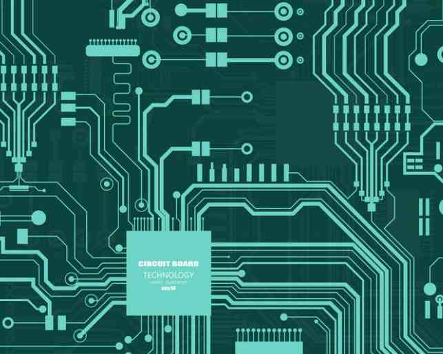
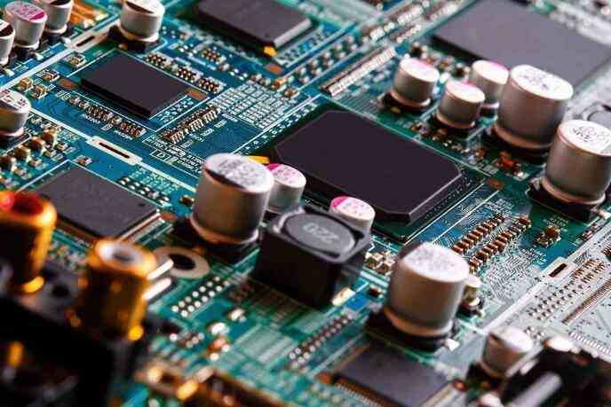
Professional PCB manufacturing and assembly
Building 6, Zone 3, Yuekang Road,Bao'an District, Shenzhen, China
+86-13410863085Mon.-Sat.08:00-20:00

pcba refersto the entire manufacturing process of pcb empty board through SMT or through DIP plug-in. Then, what processes should pcba process and make samples? This time, long Bo technology and you will introduce the pcba processing proofing process!
pcba processing and proofing process is as follows:
1. Communication, consultation and docking data.
2. Engineering process evaluation.
3. Quotation, divided into three parts: pcb board, light board, electronic components, processing fees. pcba processing is a one-stop shop that estimates all process costs from engineering documents to finished products.
4. Preparation of DFM files.
5. Purchase materials. The components are usually collected by pcba processing plant.
6. pcba proofing warehouse feeding, taking and preparing materials.
7, processing, into the production link. Including pcb proofing, SMT mounting and so on
8. Testing, including function testing, aging testing, burning testing and signal testing after pcba proofing.
9. Assembly, including single product assembly, component integration and final assembly. In this process, it is necessary to strictly control the damage caused by static electricity to the finished product that has passed the test.
Through a brief review of the whole process, I believe you have a preliminary understanding of the production process of professional pcba processing plants. Because compared with the traditional pcb processing, only more material procurement, material inspection and storage, SMT mounting and so on.
How to achieve high PCB spread rate and shorten the design time, which is a lot of people are considering the problem, this time, long Bo technology and you discuss the design skills of pcb board layout.

Layout of circuit board copying board components:
1. In the process of optimal assembly, manufacturability design rules will restrict the layout of pcb board copying components. If the assembly department allows the components to move, the circuit can be optimized for automatic wiring.
2. In the layout of pcb circuit board, the power decoupling circuit should be designed near the relevant circuit, rather than placed in the power supply part, otherwise it will not only affect the bypass effect, but also flow pulsating current above the power line and ground wire, causing interference;
3. For the power supply direction inside the circuit, power supply should be taken from the final stage to the forward stage, and the power filter capacitor of the pcb circuit board is arranged near the final stage;
4, we should pay attention to the voltage control pcb circuit board copy board power supply in the layout, as far as possible arranged in a separate printed board. When the power supply and circuit are used together in the printed board, in the layout, the voltage regulator should avoid mixing the power supply and circuit components or making the power supply and circuit common ground.
pcb circuit boards in the wet environment, easy to cause a variety of problems, such as short circuit, circuit board signal break, these faults are some. How to tell if the pcb board is wet?
Long Bo technology and share the pcb circuit board in the wet environment will appear in the problem!
If the pcb circuit board is used in a humid environment, the air in this environment contains relatively large moisture. When the moisture is too large, it will turn into water drops and fall on the pcb circuit board. After falling on the pcb circuit board, the water drops will be attached to each pin of the electronic component or the printed line.
Printed line is infiltrated by water beads, especially the signal transmission line is relatively small, after being infiltrated for a period of time, there will be printed line mold break, resulting in the circuit board at the time of work, can not run.
The reasons for the failure of the circuit board caused by moisture are classified into three categories:
1. Lead to the change of circuit parameters in pcb circuit board and lead to pcb board failure;
2. Cause the circuit of pcb circuit board to be in a short circuit state, resulting in pcb circuit board failure;
3, resulting in the pcb circuit board signal processing or transmission line break, resulting in pcb board failure.
pcb laminate pressing is a process in which one or more pieces of inner layer etched board (after black oxidation treatment) and copper foil are dipped into a multilayer board by heat curing after high temperature and high pressure semi-cured sheet. Pressing is an important process of making PCB multilayer board.
When pcb board is made, how is the multilayer board pressed?
1. Pressure cooker
This is a kind of container full of high temperature saturated water vapor, and can be applied to high pressure, pcb board production, can be laminated substrate sample, placed in it for a period of time, forcing the water into the plate, and then take out the plate sample on the surface of high temperature molten tin, measurement of its "lamination resistance" characteristics.
2. Cap pressing method
It refers to the traditional lamination method of pcb board production in the early days. At that time, the "outer layer" was made of thin single-sided copper substrate for lamination and pressing, until the production increased, the current copper type of large or mass pressing method was used.
3. Wrinkles
In the laminate pressing, often refers to the copper in the treatment of improper wrinkles.
Step 4 Dent
Refers to the production of pcb board, the copper surface of the uniform dip, may be due to the compression of the steel plate its local spot-like protruding, such shortcomings if unfortunately in the corrosion of copper is still on the line, will cause high-speed transmission signal impedance instability, and pcb board will appear noise.
Mass Lam refers to a mass-produced multilaminate, in which the outer layer of copper foil and film is pressed directly into the inner layer of skin, to become mass Lam, which replaces the earlier traditional single-sided thin substrate pressing process.
Diversification of PCB
Feb 04,2023


Just upload Gerber files, BOM files and design files, and the KINGFORD team will provide a complete quotation within 24h.